
Who are the key players and newcomers in the global IP race for the most advanced bonding technology shaping the future of semiconductor packaging?
Publication August 2024
| Download Flyer | Download Sample |
KEY FEATURES
- PDF>70 slides
- Excel file>1,600 patent families
- Global patenting trends, including time evolution of patent publications, countries of patent filings, etc.
- Main patent assignees and IP newcomers in the different segments.
- Key players’ IP position and the relative strength of their patent portfolio.
- Patents categorized by type of invention (manufacturing methods, equipment, semiconductor structures and devices) and targeted applications (image sensors, 2.5D/3D IC, 3D-stacked memories, photonics, etc.)
- IP profile of key players (patent portfolio overview, technical coverage, geographical coverage, key patents, recent IP activity, etc.)
- Excel database containing all patents analyzed in the report, including patent segmentations and hyperlinks to an updated online database, along with the complete data by assignee from the statistical analyses.
Find our related analyses in this area of advanced semiconductor packaging.
Hybrid bonding has become a key enabler of advanced packaging
Hybrid bonding combines dielectric-to-dielectric and metal-to-metal bonds to interconnect wafer-to-wafer, die-to-wafer, or die-to-die without the need for solder or other adhesives. This bonding technology is used for the vertical stacking of multiple chips, enabling 3D heterogeneous integration and interoperability of different types of chips with various functions (e.g., logic, memory, analog, sensors) within a single package. Hybrid bonding enables finer pitch (<10µm, or even <1µm) with significant benefits for interconnect density and device performance. The direct metal-to-metal contact facilitates efficient heat dissipation and reduces the parasitic delay. The dielectric insulates each metal pad so that there is no signal interference between the pads.
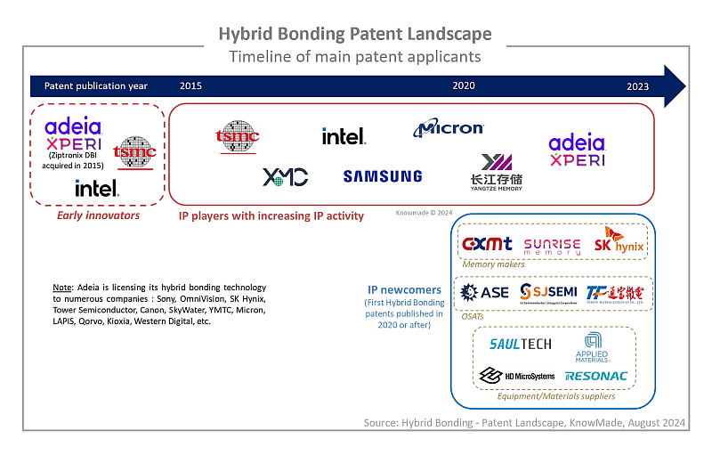
Hybrid bonding technology emerged in 2005 with the introduction of Ziptronix’s direct bond interconnect (DBI®) technology. In 2015, Tessera (now Adeia) acquired Ziptronix, and DBI® technology entered the market in 2016 through Sony’s CMOS image sensor (CIS) used in Samsung’s Galaxy S7 mobile phone. Since then, hybrid bonding technology has been explored for various applications, including memory, logic, RF, and photonics, and it is now being adopted by more companies across the semiconductor industry.
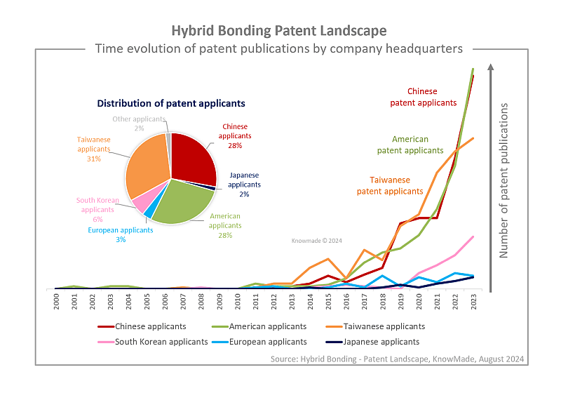
Over the past five years, hybrid bonding technology has become a key enabler of advanced semiconductor packaging, leading to a strong increase in patenting activity and a significant evolution of the competitive intellectual property (IP) landscape. Major patent owners have strengthened their IP positions in the US, China, and Europe, while various new players have entered the patent landscape. It is now crucial for companies operating in the semiconductor packaging industry to closely examine hybrid bonding technology from an IP perspective.
In this context, Knowmade is releasing a new patent landscape report focusing on the hybrid bonding process and semiconductor devices made using hybrid bonding interconnects. Over 5,800 patents from more than 1,600 patent families (inventions) have been selected. This report aims to provide insights into current IP activities, the positions of key IP players, the applications they target in their patents, and how their patent portfolios can support their market strategies.
Understanding the main trends, the key players’ IP position and IP strategy
Through patent analysis, we describe the position of IP players, unveil their strategies to strengthen their IP portfolio, highlight their capability to limit the patenting activity and freedom-to-operate of other firms, identify promising new players, and forecast what would be the future IP leaders. IP competition analysis should reflect the vision of players with a strategy to enter and develop their business in the advanced semiconductor packaging market. In this report, we provide a comprehensive overview of the competitive IP landscape and latest technological developments related to hybrid bonding technology. The report covers IP dynamics and key trends in terms of patents applications, patent assignees, filing countries, patented technologies, and targeted applications. It also identifies the IP leaders, most active patent applicants, and sheds light on under-the-radar companies and new players in this field.
 Invention type, targeted applications, and key patents
The patents have been categorized according to the type of claimed invention (hybrid bonding manufacturing methods and interface engineering, equipment for hybrid bonding technology, hybrid bonded semiconductor structures or devices) and the applications mentioned in the patents (image sensors, 2.5D/3D ICs, 3D-stacked memories, photonics, MEMS, RF, etc.). The 2.5D/3D IC segment is currently driving patenting activity, while patents related to other applications, such as photonics, microLED, MEMS, and RF, have surged.
 A dynamic IP landscape: evolution of leading players’ positions and entry of new patent applicants
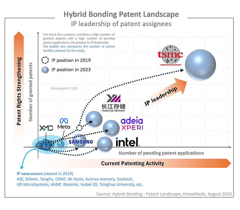
TSMC, Adeia, YMTC, Intel, and Samsung are leading the patent landscape, increasing patenting activity, and expanding invention protection in key countries. As pioneer and owner of DBI® technology, Adeia has adopted an aggressive strategy to assert its patents and license its hybrid bonding IP portfolio to various semiconductor companies, including Sony, YMTC, Micron, and Kioxia. Despite its strong IP position, other players have been developing their own hybrid bonding patent portfolios. In recent years, more memory makers have become involved in the IP landscape (CXMT, SK Hynix, Sunrise Memory), and OSATs and equipment/materials suppliers have entered the IP arena (ASE, TongFu, SJSemi, Applied Materials, Saultech, HD MicroSystems). In this report, we provide an overview of the IP portfolios held by key players and describe key patents and recent IP activities. Additionally, we highlight the main IP collaborations (co-owned patents, IP transfers, licensing agreements) and patent litigations.
Useful Excel patent database
This report includes an extensive Excel database with all patents analyzed in this study, including patent information (numbers, dates, assignees, title, abstract, etc.) and hyperlinks to an updated online database (original documents, legal status, etc.), affiliation segments (manufacturing methods, equipment, semiconductor devices, image sensors, 2.5D/3D IC, 3D-stacked memory, etc.), and key patents. Additionally, the Excel file comprises the complete data by assignee from the statistical analyses, including the number of patent families, timeline of patenting activity, number of granted patents and pending patent applications, and geographical coverage of patent portfolio.
Companies mentioned in the report (non-exhaustive)
TSMC, YMTC, Xperi/Adeia, Intel, Samsung, XMC, Micron, Tongfu Microelectronics, ASE, Meta (Facebook), Nanya Technology, CXMT, Huawei, Onsemi, OmniVision, AMD, ICLeague Technology, Monolithic 3D, UMC/Wavetek, Qualcomm, SJSemi, Saultech, SK Hynix, Tsinghua University, CEA, imec, Galaxycore Microelectronics, Apple, EVG, HD MicroSystems, NCAP, STMicroelectronics, Applied Materials, Resonac, GlobalFoundries, SunRise Memory, Alibaba Group, AP Memory, SMIC, Powerchip Semiconductor Manufacturing, MICLEDI, AMS-Osram, SmartSens Technology, Shenzhen Aoshiwei Technology, MediaTek, IBM, RTX Corporation, pSemi, Winbond electronics, Sony, NVIDIA, Haiguang Information Technology, Shanghai Huali Integrated Circuit Manufacturing, JCET Group, SEMES, Tectus Group, Hanmi, Western Digital, Shibaura Mechatronics, Ningbo Semiconductor International Corporation (NSI), HIDM – Huaian Imaging Device Manufacturer, Bruker, Suzhou Ultiview Technology, KLA, Shanghai Fudan Microelectronics Group, Anhui Xinbiyou Information Technology, Tokyo Electron, Shanghai Yibu Semiconductor, HTSI, GROQ, Dixtech innovation, Qingdao New Core Technology, PsiQuantum, Canon, Infineon, Shanghai Biren Intelligent Technology, Yangtze River Advanced Storage Industry Innovation Center, G-ray Switzerland, and more.