SOPHIA ANTIPOLIS, France – September 12, 2024 │ Artificial intelligence (AI) and high-performance computing (HPC) are considered crucial for both economic and military strength. In this context, the U.S. has implemented various restrictions on China, particularly aimed at the semiconductor industry, including limiting the sale of advanced chips and related manufacturing equipment to Chinese companies. To counteract the impact of these sanctions and advance its capability to produce cutting-edge chips, China is pursuing alternative strategies, with a particular emphasis on developing its advanced semiconductor packaging technologies and related intellectual property (IP).
Chinese companies are increasingly investing in hybrid bonding intellectual property to strengthen their advanced semiconductor packaging technologies
Patent analytics reveal a boom of patent publications related to advanced packaging worldwide (Figure 1). Among the key technologies, hybrid bonding has experienced the strongest acceleration in patent filings. This bonding process involves connecting chips/wafers without solder balls, combining both direct metal-to-metal and oxide-to-oxide bonding. The advantages include a higher interconnect density, faster signal transmission, lower power consumption, improved heat dissipation, and 3D heterogeneous integration. As a result, hybrid bonding has raised the interest of semiconductor companies globally, including those in China (Figure 2). As pioneer, Adeia (formerly Xperi) acquired the direct bond interconnect (DBI®) technology from Ziptronix in 2015 and has been licensing it to various companies, including Sony, YMTC, Micron, and Kioxia, ever since. TSMC and Intel have also invested in R&D efforts from the early days in this cutting-edge bonding technology, developing their own IP portfolios and advanced packaging innovations for chiplets, such as TSMC‘s 3D-stacked System-on-Integrated Chips (SoIC) and Intel’s Foveros Direct. After DBI® technology entered the image sensor market in 2016 through Sony’s CMOS image sensor in Samsung’s Galaxy S7, memory makers like Micron, Samsung, and YMTC joined the IP race. Beyond memory applications, hybrid bonding has become essential for achieving the most advanced packaging capabilities. Consequently, China is investing heavily in this technology, with YMTC and XMC increasing their hybrid bonding-related patenting activities, while TongFu Mircroelectronics, SJSemi, and CXMT have entered the hybrid bonding IP landscape over the last 3 years.
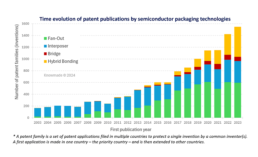
Figure 1: Time evolution of the main technologies related to advanced packaging (Source: Hybrid Bonding Patent Landscape report, Knowmade, September 2024).
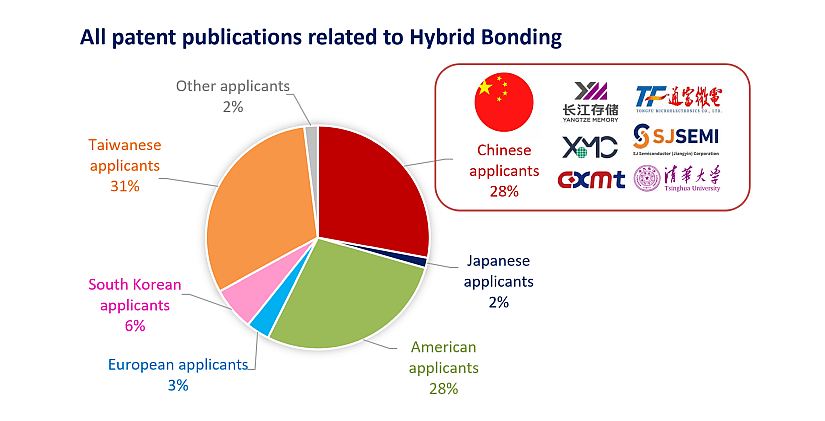
Figure 2: Overview of the headquarters of companies publishing patents related to hybrid bonding (Source: Hybrid Bonding Patent Landscape report, Knowmade, September 2024)
TongFu’s patenting activity related to hybrid bonding
TongFu MicroElectronics, formerly known as Nantong Fujitsu Microelectronics (NFME), has a long-standing presence in the advanced semiconductor packaging industry. Patent analysis reveals that the company has been active in the Fan-Out packaging field since 2011, with a significant acceleration in patent filings in 2022. It now rivals with other outsourced semiconductor assembly and testing (OSAT) companies like JCET, ASE, SPIL, Huatian, and SJSemi in this Fan-Out IP landscape. Since 2022, TongFu has ventured into the hybrid bonding IP landscape, with over 30 pending patent applications to date. Its claimed inventions are primarily related to semiconductor structure/device fabrication, integrating hybrid bonding as one of the steps rather than focusing on the hybrid bonding process itself. While most patent applications are filed in China, the company has shown interest in enforcing its legal rights in Europe, as evidenced by at least four patent filings targeting Europe through ongoing PCT procedures (WO2023/104092, WO2023/104094, WO2023/104095, WO2023/104097). TongFu‘s hybrid bonding IP strategy appears to mirror its approach in the Fan-Out segment, with most patents being filed in China and only a few directed towards other countries, specifically Europe and the U.S.
Hybrid bonding technology has become crucial for 2.5D/3D Fan-Out packaging and 3D-stacked memory developed by TongFu. Most of its patents describe techniques for fan-out packaging which involve hybrid bonding technology for stacking multiple chips (WO2023/104094, WO2023/104097, CN115527868, CN114188316, CN115732475). The inventions propose combining dummy chips, conductive through holes, and silicon interposers with wafer-level hybrid bonding techniques to achieve high-density, ultra-thin, multi-layer chip packages. The solutions described in these patents enhance mechanical stability, prevent warping, and reduce package thickness while improving electrical performance and heat dissipation. By integrating heterogeneous chips efficiently, TongFu’s claimed inventions also increase packaging versatility and reliability. Regarding the high-bandwidth memory (HBM), TongFu utilizes hybrid bonding to vertically stack memory chips and mount the 3D-stacked memory onto a substrate (WO2023/104092, CN114464542, CN114203564, CN114171414). These inventions propose combining advanced solutions such as hybrid bonding with dummy and buffer chips, conductive through holes, and heat dissipation structures, all aimed at improving data throughput, thermal management, and mechanical stability in memory packages. The resulting benefits include higher memory capacity, increased data transfer rates, and enhanced reliability, all within a more compact and efficient package. Additionally, another patent discloses a method for separating a hybrid bonding wafer, which allows the separation of adjacent chip sets without damaging the hybrid bonding interface (CN114758952). The method involves dry etching along a specific direction from both sides of the wafer assembly to create grooves that intersect with the hybrid bonding interface.
TongFu’s IP signals a strong drive towards high-end semiconductor packaging
TongFu’s intellectual property, which combines hybrid bonding technology with fan-out packaging and 3D memory stacking, gives the company a significant advantage in assembling semiconductor devices with higher integration density, performance, and energy efficiency. The development of a patent portfolio related to hybrid bonding, coupled with its joint venture and strategic partnership with AMD, supports TongFu’s ambition to advance in the fabrication of high-performance semiconductor packaging for premium applications, such as AI and HPC, where faster processing speeds and increased data capacity are critical.
Press contact
contact@knowmade.fr
Le Drakkar, 2405 route des Dolines, 06560 Valbonne Sophia Antipolis, France
www.knowmade.com
About the author
Pauline Calka, PhD. works for KnowMade as a patent analyst in the fields of semiconductor manufacturing and advanced packaging. She holds a PhD in Memory from the University of Grenoble Alpes (France), in partnership with the CEA-Leti (France). After an Alexander von Humboldt Postdoc fellowship position at the Technical University of Berlin (Germany) and the Leibniz Institute for High Performance Microelectronics on ReRAM development, Pauline worked five years at ASM International (Belgium) as Senior Process Engineer on thin film development for logic, memory and MEMS, and two years at CEA-Leti as Integration Engineer on imaging CMOS sensors.
About KnowMade
KnowMade is a technology intelligence and IP strategy consulting company specialized in analyzing patents and scientific publications. The company helps innovative companies, investors, and R&D organizations to understand competitive landscape, follow technological evolutions, reduce uncertainties, and identify opportunities and risks in terms of technology and intellectual property.
KnowMade’s analysts combine their strong technology expertise and in-depth knowledge of patents with powerful analytics tools and methodologies to turn patent information and scientific literature into actionable insights, providing high added value reports for decision makers working in R&D, innovation strategy, intellectual property, and marketing. Our experts provide prior art search, patent landscape analysis, freedom-to-operate analysis, IP due diligence, and monitoring services.
KnowMade has a solid expertise in Compound Semiconductors, Power Electronics, Batteries, RF Technologies & Wireless Communications, Solid-State Lighting & Display, Photonics, Memories, MEMS & Sensors, Semiconductor Packaging, Medical Devices, Medical Imaging, Microfluidics, Biotechnology, Pharmaceutics, and Agri-Food.