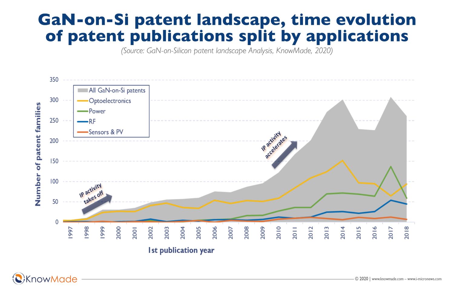
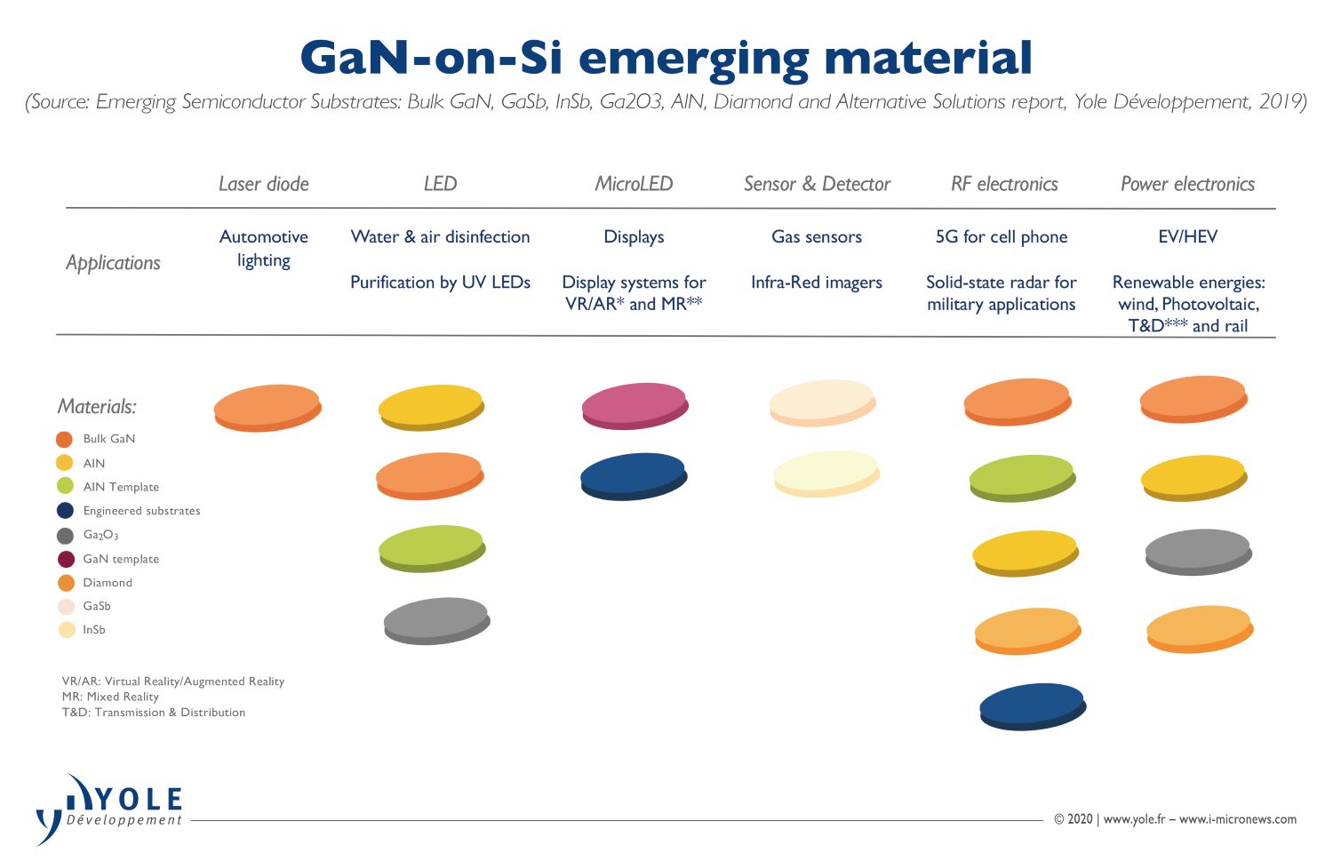
SOPHIA ANTIPOLIS, France – January 24, 2020 | “2015-2020 period has shown tremendous and decisive changes within the GaN-on-Si landscape, especially the strategy of players involved” affirms Nicolas Baron, CEO and Co-founder of KnowMade. He adds: “For example, Toshiba’s withdrawal from white LED market and the acquisition of IR by Infineon Technologies in 2015”.
OUTLINES:
– GaN-on-Si IP landscape: historical players stepping back, leading to a substantial reconfiguration of the ecosystem.
– Emerging applications in optoelectronics & photonics are driving the IP activity.
– RF electronics: Macom and Intel have taken the lead on GaN-on-Si RF technology.

At that time, Toshiba and IR were already leading the GaN-on-Si patent landscape, while several historical IP players including Panasonic, Sanken Electric, Toyoda Gosei, etc. had already slowed down their patenting activity in this field. Furthermore, after IR, Transphorm, Panasonic and GaN Systems started sampling/commercializing their first GaN-on-Si power devices between 2010 and 2015, a second wave of companies has entered the playground in the last few years: ON Semiconductor, Dialog, Navitas, VisIC. More companies, such as STMicroelectronics, are expected soon, demonstrating the growing interest for GaN-on-Si technology in the power electronics business.
Yole Group of Companies, including Yole Développement, KnowMade and System Plus Consulting, are deeply engaged in the analysis of the overall GaN industry. The three companies are working together day by day to get a deep understanding of the market and its status. They follow innovations, evaluate their impact on the market and analyze the strategy of the leading players. Their aim is to get a comprehensive overview of the transformation of this industry.
Today, KnowMade announces its patent landscape analysis focused on GaN-on-Si technologies: GaN-on-Silicon Patent-Landscape Analysis. This report enlarges the collection of reports performed by Yole Group of Companies in this domain. It is part of the full GaN reports collection, including today, Power GaN: Epitaxy, Devices, Applications & Technology Trends, RF GaN Market: Applications, Players, Technology and Substrates and MicroLED Displays from Yole, RF GaN – Patent Landscape Analysis, Power GaN – Patent Landscape Analysis and GaN Power & RF – Patent Monitoring Service from KnowMade, and Medium Voltage GaN HEMT vs Superjunction MOSFET Comparison from System Plus Consulting.
In addition, the Group proposes a special focus on the power electronics industry with a dedicated online event on January 30: “First Milestone for GaN Power Devices”. This webcast powered by Yole, System Plus Consulting and KnowMade is a great opportunity to understand and get a better vision of the GaN ecosystem and its supply chain, collect market figures and trends and discover a spotlight on the IP strategy of the key players.
“Intel and Macom are leading the GaN-on-Si patent landscape for RF electronics applications” says Remi Comyn, PhD, Compound Semiconductors and Electronics at KnowMade.
Intel’s RF GaN-on-Si patent portfolio mainly relates to III-N transistors used in SoC , RF switches, ultra-short channel lengths, field plates, and III-N/Silicon monolithic IC . Still, about 75% of Intel’s portfolio are composed of pending patent applications distributed mainly between USA with 17 patents and Taiwan with 20 patents.
Fujitsu with more than 40 patents and Macom with more than 20 patents for its side, are leading the patent landscape in terms of enforceable IP in the field of GaN-on-Si RF. Fujitsu’s portfolio focused on GaN-on-Si materials, especially on buffer layers, with inventions that might be implemented on others substrates including SiC or for other applications. Likewise Intel, Fujitsu has adopted a global patenting strategy. In contrast Macom’s portfolio is more focused on GaN-on-Si devices for RF, addressing specific technological challenges at epitaxy, device, module and package levels. For instance, a strong patenting effort was made in 2015 in order to address the parasitic channel via counter dopants in HEMT epi-structures. KnowMade’s analysts identified more than 10 related patent applications in its new GaN-on-Silicon patent analysis. Furthermore, Macom’s patenting activity related to GaN-on-Si is essentially focused on US, although it has now requested foreign extensions for a significant number of newly published inventions.
Regarding the power electronics field, Rémi Comyn from KnowMade comments: “The growing interest in GaN-on-Si technology for power applications has not translated into a remarkable acceleration of the patenting activity. However, we observed a steady patenting activity from Infineon following IR’s acquisition, and a remarkable strengthening of Transphorm’s portfolio after Fujitsu’s decision to transfer its power supplies businesses to the US startup”.
Transphorm’s IP position has been further reinforced following the licensing agreement established in 2014 with Furukawa Electric, a key IP player in GaN-on-Si patent landscape. Likewise, Infineon Technologies closed an important IP licensing agreement with another historical player of GaN-on-Si and power electronics patent landscapes, Panasonic. Furthermore, KnowMade will keep monitoring closely GaN-on-Si IP activity in the next month, since another major power electronics player.
STMicroelectronics, announced in 2018 an extensive R&D program in collaboration with CEA Leti a well-positioned player in the GaN-on-Si patent landscape.
From a technical point of view, Ezgi Dogmus, PhD, Technology & Market Analyst Compound Semiconductors & Emerging Materials at Yole asserts: “Over the last years, in the power electronics industry, we have witnessed an increasing interest for GaN HEMTs, which bring attractive performance and cost-competitive compared to Si MOSFETs. In addition to innovative start-up companies, almost all integrated device manufacturers in the Power Electronics business propose currently GaN-on-Si devices enabling systems with higher power, higher efficiency and smaller foot print than their Si MOSFET solutions.”
In power electronic sector, GaN -on-Si devices are direct competitors of Silicon SJ MOSFETs at medium voltage.
“SJ MOSFETS are still cost effectives and technologically interesting” explains Elena Barbarini, Head of Department Devices at System Plus Consulting. “But the increase of players as the development of attractive performances at GaN epitaxy level drove an acceleration of available solutions. Its regards die design, driver integration and packaging.” This competition is analyzed in details the Medium Voltage GaN HEMT vs Superjunction MOSFET Comparison report performed by System Plus Consulting.
After a spotlight highlighting the GaN-on-Si patent activities in RF and Power electronics sectors, another interesting application has to be pointed out. Indeed, the increasing GaN-on-Si activity within the microLED activities is step by step becoming more attractive and leads to huge volume opportunities.
As of 2019, a significant contribution to the patenting activity (in terms of new inventions) stems from the development of a low cost and scalable GaN-on-Si nanowires-based microLED technology, which are promising for the next-generation display technology and smart lighting applications. Most microLEDs related patents included in the landscape are related to the fabrication of GaN nanostructures.

Eric Virey, PhD, Principal Analyst, Technology & Market, Displays at Yole tells us the story: “The technology was first developed and patented by glō between 2010 and 2016. However, glō’s patenting activity does not put the emphasis on GaN-on-Si, although it is a preferred embodiment”. For more information about glō’s developments, discover its interview conducted by Eric Virey and published on i-Micronews.
In parallel, since 2014, CEA and Aledia started patenting their own – jointly developed – technology with numerous requests for extending its priority patents worldwide indicating a global IP strategy/competition.
In this dynamic ecosystem, GaN-on-Si technologies look attractive and promising. This phenomenon is highlighted with the numerous patents incoming. Under this context, KnowMade, as a technology intelligence and IP strategy consulting company specialized in the analysis of patents and scientific information, and its partners, Yole and System Plus Consulting will pursue their investigations in this field and keep you update about the latest technical innovations, patents and industrial news.
Patent landscape reports dealing with Power electronics.
Press contact
contact@knowmade.fr
Le Drakkar, 2405 route des Dolines, 06560 Valbonne Sophia Antipolis, France
www.knowmade.com
About Knowmade
Knowmade is a Technology Intelligence and IP Strategy consulting company specialized in analysis of patents and scientific information. The company helps innovative companies and R&D organizations to understand their competitive landscape, follow technology trends, and find out opportunities and threats in terms of technology and patents.
Knowmade’s analysts combine their strong technology expertise and in-depth knowledge of patents with powerful analytics tools and methodologies to turn patents and scientific information into business-oriented report for decision makers working in R&D, Innovation Strategy, Intellectual Property, and Marketing. Our experts provide prior art search, patent landscape analysis, scientific literature analysis, patent valuation, IP due diligence and freedom-to-operate analysis. In parallel the company proposes litigation/licensing support, technology scouting and IP/technology watch service.
Knowmade has a solid expertise in Compound Semiconductors, Power Electronics, Batteries, RF Technologies & Wireless Communications, Solid-State Lighting & Display, Photonics, Memories, MEMS & Solid-State Sensors/Actuators, Semiconductor Manufacturing, Packaging & Assembly, Medical Devices, Medical Imaging, Microfluidics, Biotechnology, Pharmaceutics, and Agri-Food.
