August 25, 2022

KnowMade’s expertise in semiconductor packaging

Advanced packaging techniques as promising solutions to fulfill the needs of the semiconductor industry

The demand for constantly evolving semiconductor technologies remains high in the market, but Moore’s Law becomes increasingly difficult to achieve as node advancement reaches its limits, further scaling in advanced nodes being hardly cost-effective. As a result, the process of chip miniaturization has been slowing down and the semiconductor industry is facing a gap in technology advancement. Advanced packaging techniques, such as 2.5D, 3D, and fan-out wafer level packaging, have emerged as promising solutions to fill the gap and meet the needs of the semiconductor market. These new approaches allow for the integration of multiple dies into a single package, with the possibility of combining mature and advanced nodes.

The growth of the System-in-Package (SiP) market is driven by the 5G, artificial intelligence (AI), high-performance computing (HPC), autonomous driving, and Internet-of-Things (IoT) segments. While the semiconductor packaging market primarily uses flip-chip (FC) and wire-bond (WB) technologies, there is an increasing demand for integrating more components into a SiP in order to achieve smaller form factors and higher performance products.

There are competing interests between the cost increase per yielded mm2 of silicon leading-node technology and the insatiable demand for more compute and memory per package. The solution is more die connected with interconnect technologies. In order to address this issue, the semiconductor industry must employ more advanced interconnect technologies, such as Si interposers, embedded bridges, UHD RDLs, and others, as well as implement more vertical connections using TSVs, micro-bumps, Cu posts, bumpless Cu/SiO2 hybrid bonding, RDL vias, etc.

Challenges for packaging technologies

Three main advanced packaging technologies – wafer level packaging (WLP), 2.5D, and 3D stacking – have supplemented the dominant flip-chip and wire-bond technologies. The roadmap for these technologies is challenging and the supply chain is becoming increasingly competitive, with the demand for high-density fan-out (HD FO) redistribution layers (RDLs), high-density input/output interconnections (I/O) that require smaller line/space (L/S) patterns, and advanced 2.5D/3D packaging techniques such as silicon interposer and embedded bridge. Heterogeneous integration and chiplets are pushing for more complex system-in-package (SiP) solutions to be adopted. Chiplet-based approach offer smaller SiP footprints with lower power consumption and facilitate the integration of multiple dies using various interconnect methods such as high-density substrates, interposers, bridges, and hybrid bonding.

The market for 2.5/3D packaging is showing the most potential for growth. Currently, the highest revenue contributors are stacked CMOS image sensors (CIS) and silicon interposers. However, the technology with the most rapid growth is 3D SoC, driven by the trend of hybrid bonding for chiplets 3D integration. The partitioning of large dies into chiplets and heterogeneous integration are also important market trends that are driving the development of Fan-Out packaging. High density fan-out (HD FO) is currently the dominant market class, but the ultra-high density fan-out (UHD FO) is the highest-growing segment that will take market share from silicon interposers in the future with innovative FO-on-substrate and FO-embedded-bridge solutions.

Semiconductor packaging was primarily performed by outsourced semiconductor assembly and test companies (OSATs) such as ASE/SPIL, Amkor, JCET, etc. These companies continue to play an important role in this field, but it is TSMC, Samsung and Intel that have been offering advanced back-end solutions and using their front-end capabilities to develop innovative 2.5D/3D packaging solutions such as silicon interposer, embedded bridge, and hybrid bonding.

KnowMade’s purpose

KnowMade’s semiconductor packaging team offers a unique and valuable understanding of the latest innovations and ecosystem evolution in advanced packaging through patent analysis reports and monitoring services. Our analysts track and analyze the patent activity of leading companies, such as TSMC, Samsung, Intel, Amkor, ASE, SPIL, JCET, Nepes, PTI, Deca, Huatian, TFME, SJSemi, SK Hynix, Xperi, and others. We can provide insights into their technology roadmap and IP strategy, particularly in high-end performance packaging, including UHD Fan-Out, 2.5D silicon interposer or embedded bridge, 3D stacking of dies, and hybrid bonding.

Our packaging analysts pay special attention to the following technologies:

  • Fan-Out packaging: fan-out wafer level packaging (e.g., Infineon’s eWLB, TSMC’s InFO, ASE’s FOCoS, etc.), fan-out panel level packaging (e.g., PTI’s CHIEFS, CLIP, PiFO, and BF2O, etc.), redistribution layers (RDL), chip-first / RDL-first, single-chip FO / multi-chip FO, FO-on-substrate, FO interconnect bridge, 3D multi-stack FO (stacked die, SoCs & memory integration), FO package-on-package (FO-PoP), FO antenna-in-package (FO AiP), etc.
  • 2.5D packaging: silicon interposer (e.g., TSMC’s CoWoS-S, Intel’s Foveros, Samsung’s H-Cube and I-Cube), embedded silicon bridge (e.g., Intel’s EMIB and Co-EMIB, TSMC’s CoWoS-L and InFO_LSI, ASE’s FOCoS-Bridge), redistribution layers (e.g., TSMC’s CoWoS-R), glass interposer, etc.
  • 3D packaging: 3D system-on-chip (3D SoC), 3D integrated circuit (3D IC), 3D stacked memory (e.g., HBM, 3D stacked DRAM, 3D NAND stack), TSV with µbumps/Cu pillars, bumpless hybrid bonding (e.g., Xperi’s DBI, TSMC’s SoIC, Intel’s Foveros Direct, YMTC’s Xtacking), 3D Fan-Out, 3D heterogeneous integration, chiplets, etc.

Latest reports on semiconductor packaging

Featured image of Hybrid Bonding Patent Landscape Analyses 2024.
Who are the key players and newcomers in the global IP race for the most advanced bonding technology shaping the future of semiconductor packaging? Publication [...]
Major companies have patented variety of solutions to protect their own AiP structures and manufacturing processes. What are the white spaces left? Is the freedom [...]
    KnowMade has just published a new report, updating this analysis in 2024. Follow this link to discover it: Hybrid Bonding Patent Landscape 2024. [...]

Patent monitors on semiconductor packaging

Featured image of Advance Packaging monitor.
Get up-to-date data on Advanced Semiconductor Packaging patent activity: New patent applications, patents newly granted, expired or abandoned patents, latest patent transfers, patent litigations and [...]

Latest insights on semiconductor packaging

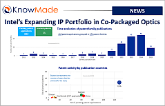
Featured image of the article Intel’s Expanding IP Portfolio in Co-Packaged Optics.
SOPHIA ANTIPOLIS, France – November 13, 2025 │ As demand for data-intensive computing continues to rise, Intel has developed an extensive suite of patents addressing [...]
Featured image of the article YMTC’s Hybrid Bonding Patents: A Key Competitive Factor for Memory Chipmakers.
SOPHIA ANTIPOLIS, France – June 19, 2025 │ Hybrid bonding is a technique that connects two semiconductor chips by directly bonding copper interconnects to copper [...]
Featured image of the article Pure Player Lightmatter is Securing Optical Interposer Intellectual Property Shares.
SOPHIA ANTIPOLIS, France – April 07, 2025 │ Optical interposers are a crucial technology for advanced semiconductor packaging and co-packaged optics, driving the rapid growth [...]

November 13, 2025

Intel’s Expanding IP Portfolio in Co-Packaged Optics

SOPHIA ANTIPOLIS, France – November 13, 2025 │ As demand for data-intensive computing continues to rise, Intel has developed an extensive suite of patents addressing the integration of photonic and electronic systems at the package level. These inventions collectively illustrate the transition from traditional electrical interconnects toward optical input/output (I/O) architectures that enable higher bandwidth, lower latency, and improved energy efficiency across compute and networking platforms. This article focuses on Intel’s strategy and key innovations in co-packaged optics (CPO) and optical interconnects (optical I/O), ahead of our upcoming advanced packaging intellectual property (IP) landscape report that will provide an overview of the patent activity and strategies of the key players in this field.

A patent-powered shift: Intel’s road to co-packaged optics and optical I/O

At the 2024 Optical Fiber Communication conference, Intel’s Integrated Photonics Solutions group unveiled a prototype Optical Compute Interconnect (OCI) chiplet, a fully integrated optical I/O device co-packaged with a CPU and transmitting live data. Demonstrating 4 Tb/s of bidirectional throughput at approximately 5 pJ/bit, the prototype underscored Intel’s progress toward scalable, energy-efficient optical interconnects designed to meet the extreme bandwidth and power demands of AI infrastructure and high-performance data centers. Although still at the prototype stage, the OCI marked a decisive step toward unifying photonics and electronics within a single computing package, a convergence widely regarded as essential for overcoming the limitations of copper-based interconnects. By moving optical I/O closer to the processor, Intel aims to reduce latency, power consumption, and signal loss while dramatically increasing interconnect density, a foundational advance for future heterogeneous computing systems.

Intel’s live demonstration provides a tangible glimpse into its long-term vision: the transition from pluggable optical transceivers toward tightly co-packaged, light-based interconnects. This shift reflects broader trends across the semiconductor industry, where the integration of optical components directly into compute packages is seen as a path to sustained performance scaling. The OCI prototype therefore serves not just as a proof of concept, but as a technological marker for Intel’s broader roadmap, one that blends advances in silicon photonics, advanced packaging, and thermal co-design to redefine how data moves within and between compute systems.

A patent landscape of integrated photonics innovation

Beneath public communications lies an extensive and evolving patent portfolio that maps Intel’s strategic progress in photonic-electronic integration. These patents reveal a systematic effort to merge optics, electronics, packaging, and thermal management across multiple levels of integration, from on-package optical I/O and co-packaged opto-electronic assemblies to emerging glass interposers and embedded cooling architectures. Viewed collectively, these inventions trace Intel’s trajectory from early optical interconnect research toward a comprehensive platform strategy that unites photonics and silicon computing. They illustrate a clear shift away from discrete optical modules toward dense, light-enabled interconnect fabrics that could transform system-level performance, efficiency, and scalability.

Over the past five years, the semiconductor company has shown a strong upward trend in patenting activity. Its robust and expanding IP portfolio reflects a dynamic innovation pipeline, with numerous pending applications filed across major markets, particularly the US, Europe, and China (figure 1).

This technological and intellectual property evolution highlights how Intel is positioning itself at the forefront of the next computing paradigm; one where light is not merely a transmission medium, but an integral component of data processing itself.

Two graphs showing, the first, the time evolution of patent familiy publication, the second, the patent activity by publication countries, from Intel for co packaged optics.

Figure 1: Time evolution of patent family publications and geographical distribution of granted patents and pending applications from Intel for co-packaged optics and optical interconnects. Note: The data corresponding to the year 2025 is not complete since the patent search was done in June 2025.

1. Co-packaged opto-electronics: Vertical integration at the system level

Intel addresses data center networking challenges in patent US11217573 (figure 2), which describes a network switching package optimized for high-bandwidth photonic integration. The patent proposes stacking photonic engines (320) on both the top and bottom surfaces of the package substrate (305), thereby doubling available bandwidth without expanding the footprint. Sockets with extended stand-off heights create space below the interposer for thermal management and optical coupling, minimizing signal loss and improving power efficiency. This vertically integrated structure enables scalable bandwidth density for next-generation network switches, achieving higher total throughput within the same footprint.

Schema abstracted from Intel patent.

Figure 2: Stacked photonic engines in network switching package (Intel, US11217573).

2. Co-packaged opto-electronics: Optical I/O at the processor level

The patent US9507086 (figure 3) details one of Intel’s foundational approaches to on-package optical integration. Here, lasers, modulators, photodetectors, and couplers are mounted directly onto the processor substrate, enabling optical signals to communicate with the processor without intermediate electrical conversions. This reduces latency, increases aggregate bandwidth, and improves energy-per-bit performance, all while maintaining compatibility with existing CMOS fabrication and packaging methods. This patent establishes Intel’s early and continuing leadership in bringing optical interconnects directly onto processor packages, transforming compute fabrics for AI and cloud-scale workloads.

Sketch from an Intel's patent.

Figure 3: Processor-level optical integration with on-package lasers and modulators, for electrical free I/O (Intel, US9507086).

Patent US12266608 (figure 4, left) introduces a co-packaged design that directly integrates a heterogeneous processing unit (XPU) with a photonic integrated circuit (PIC) using Intel’s Embedded Multi-die Interconnect Bridge (EMIB). The design employs fan-out redistribution layers (FORDL) to electrically couple the XPU and PIC through the EMIB, extending signal reach without performance degradation. This arrangement supports optical I/O within a single package, delivering ultra-high bandwidth over optical links, beyond the limits of electrical traces. The approach combines compact packaging and scalable optical interconnects, enabling efficient on-package photonics for HPC and data center applications.

Expanding on this concept, the patent application US20230090863 (figure 4, right) presents an optical fanout interposer architecture aimed at directly coupling XPUs with PICs through integrated waveguides (120–122). These waveguides form an “optical interposer” layer that connects logic and photonic dies with minimal electrical path length. The design supports bandwidths exceeding one petabyte per second through dense passive optical routing, while passive alignment of components simplifies manufacturing and improves yield. The resulting structure achieves extremely high data density and low-latency photonic communication, representing a major step toward disaggregated compute architectures interconnected by light.

Two abstracts from Intel's patents.

Figure 4: Left – EMIB-based co-packaged XPU–PIC integration (Intel, US12266608); Right – Optical fanout interposer with embedded waveguides (Intel, US20230090863).

3. Glass substrates: Toward optical interposers

To meet interconnect density and integration requirements beyond the limits of silicon, Intel has pioneered the use of glass substrates and hybrid bonding as the foundation for scalable opto-electronic packaging. These approaches offer improved planarity, reduced loss, and greater dimensional stability for complex optical-electrical assemblies.

Patent application US20240178207 (figure 5) introduces a glass-core interposer (103) incorporating through-glass vias (TGVs 110) that transmit both electrical and optical signals. Waveguides embedded within the glass allow for high-bandwidth optical transmission, while TGVs provide fine-pitch electrical connectivity (2–70 µm). By hybrid bonding a photonic integrated circuit to the glass substrate, optically through one portion of its active surface and electrically through another, the design achieves tight optical alignment and high interconnect density in a compact footprint. This architecture bridges the gap between traditional electrical interposers and optical interconnect layers, offering an elegant path toward glass-based optical interposers for scalable data communication modules.

A sketch of a glass core interposer from an Intel's patent.

Figure 5: Glass-core interposer with through-glass vias (Intel, US20240178207).

Similarly, the patent US12147083 describes a hybrid manufacturing process where electronic and photonic structures are bonded into a unified microelectronic assembly. The approach allows ICs containing optical elements (waveguides, modulators, or lenses) to be bonded with electronic dies containing transistors or interconnects, forming a heterogeneous stack. Additional photonic or electronic features, such as conductive vias or dielectric waveguides, can be fabricated post-bonding to enhance performance. This flexibility allows seamless photonic-electronic integration and scalability across different process technologies. In application US20230093438, Intel extends glass-based packaging to PIC-to-PIC optical communication. Photonic dies are mounted onto a glass substrate containing passive glass waveguides that provide low-loss optical links between disaggregated dies or off-package components. The architecture supports high signaling frequencies and long-reach optical channels with minimal loss, enabling direct optical communication across multi-die systems.

Combined, these patents underscore Intel’s transition from silicon interposers to glass-based, hybrid-bonded photonic platforms, a key enabler for future exascale computing and disaggregated chiplet architectures.

4. Integrated thermal management in photonic–electronic packaging

As co-packaged optics evolve toward higher power densities and denser integration, thermal management has emerged as one of the most critical challenges to reliable operation. Intel’s patents in this area reveal a multi-faceted strategy that integrates heat spreading, power delivery, and mechanical support directly into the package architecture.

Patent application US20220413236 (figure 6, left) introduces a thermally conductive, electrically active “thermal die” (330) positioned above the photonic integrated circuit (308). This thermal die provides a dual function: delivering electrical power from the substrate to the PIC while simultaneously extracting heat from localized hot spots, especially from on-chip lasers. The heat is transferred to an integrated heat spreader (324), eliminating the need for TSVs or wire bonds and simplifying assembly. This multifunctional structure enhances power delivery efficiency, thermal performance, and reliability while maintaining a compact form factor suitable for co-packaged optical engines.

Complementary to this, US20250110301 (figure 6, right) tackles the thermal bottlenecks that occur when a PIC is placed between an electronic integrated circuit and the package lid. The patent application introduces thermal plugs embedded within the PIC’s dielectric layers that connect high-heat regions directly to the substrate. These high-conductivity plugs efficiently transfer heat from both the PIC (204) and adjacent EIC dies (202, 208, 206), maintaining temperature uniformity and operational stability under heavy load. The arrangement minimizes thermal gradients and ensures reliable long-term performance for high-speed optical-electronic modules.

A sketch abstracted from an Intel's patent on co packaged optics.

Figure 6: Thermal die and plug-based cooling for PIC/EIC packages (Intel, US20220413236, left image; Intel, US20250110301, right image).

Through these innovations, Intel addresses the intertwined issues of thermal and electrical co-design in optical packaging. The introduction of integrated thermal dies and embedded thermal plugs reflects a holistic strategy that links cooling, power, and packaging, a necessary step toward practical, large-scale deployment of co-packaged optical systems.

Conclusion

Intel’s patent portfolio reveals a unified strategy to merge photonics and electronics across every level of system design. From vertically integrated network packages that increase bandwidth density without increasing footprint, to processor-level optical I/O, glass-based interposers, and integrated thermal solutions, these innovations collectively redefine how data, power, and heat are managed within high-performance systems. The progression reflects a decisive shift away from discrete optical modules toward compact, light-enabled interconnect fabrics that deliver exceptional bandwidth efficiency and scalability. Together, these advances illustrate Intel’s drive to establish photonic–electronic integration as the cornerstone of next-generation AI, cloud, and data-center computing.

While Intel’s innovations clearly position the company as a leading force in the transition toward photonic-electronic integration, it is far from alone in shaping this technological revolution. Other key IP players are also investing heavily in co-packaged optics and optical interconnect technologies. Our forthcoming advanced packaging IP landscape report on CPO & Optical I/O will examine their patent portfolios and strategies, offering a comprehensive view of the competitive ecosystem driving the next generation of optical connectivity.


Press contact
contact@knowmade.fr
Le Drakkar, 2405 route des Dolines, 06560 Valbonne Sophia Antipolis, France
www.knowmade.com

About the author
Pauline Calka, PhD. works for KnowMade as a patent analyst in the fields of semiconductor manufacturing and advanced packaging. She holds a PhD in Memory from the University of Grenoble Alpes (France), in partnership with the CEA-Leti (France). After an Alexander von Humboldt Postdoc fellowship position at the Technical University of Berlin (Germany) and the Leibniz Institute for High Performance Microelectronics on ReRAM development, Pauline worked five years at ASM International (Belgium) as Senior Process Engineer on thin film development for logic, memory and MEMS, and two years at CEA-Leti as Integration Engineer on imaging CMOS sensors.

About KnowMade
KnowMade is a technology intelligence and IP strategy firm specializing in the analysis of patents and scientific publications. We assist innovative companies, investors, and research organizations in understanding the competitive landscape, anticipating technological trends, identifying opportunities and risks, improving their R&D, and shaping effective IP strategies.
KnowMade’s analysts combine their strong technology expertise and in-depth knowledge of patents with powerful analytics tools and methodologies to transform patent and scientific data into actionable insights to support decision-making in R&D, innovation, investment, and intellectual property.
KnowMade has solid expertise in Semiconductors and Packaging, Power Electronics, Batteries and Energy Management, RF and Wireless Communications, Photonics, MEMS, Sensing and Imaging, Medical Devices, Biotechnology, Pharmaceuticals, and Agri-Food.

June 19, 2025

YMTC’s Hybrid Bonding Patents: A Key Competitive Factor for Memory Chipmakers

SOPHIA ANTIPOLIS, France – June 19, 2025 │ Hybrid bonding is a technique that connects two semiconductor chips by directly bonding copper interconnects to copper and insulating materials to insulating materials. Unlike conventional chip-stacking methods that rely on solder balls or bumps, hybrid bonding enables thinner packaging while improving both electrical and thermal performance.

Over the past five years, hybrid bonding technology has emerged as a key enabler of advanced semiconductor packaging. Driven by the aggressive R&D efforts of global semiconductor companies, the number of hybrid bonding-related patents has increased more than fourfold since 2019, accompanied by a significant transformation of the competitive intellectual property (IP) landscape. In our latest Hybrid Bonding Patent Landscape report, we identified TSMC, Adeia, and Yangtze Memory Technologies Corp (YMTC) as leading players in hybrid bonding IP.

Hybrid bonding technology has a wide range of applications. In the memory sector, it is expected to be implemented in next-generation high-bandwidth memory (HBM) with more than 20 stacked layers, 3D DRAM, and NAND flash with over 400 layers. In fact, hybrid bonding has already been commercialized in the NAND market. Chinese chipmaker YMTC has been mass-producing NAND chips using this technology, marketed as “Xtacking”, for about four years. This process involves wafer-to-wafer (W2W) bonding, where the core components of NAND (the cell and peripheral circuits) are fabricated separately on different wafers and then bonded together.

YMTC’s patent portfolio is particularly noteworthy. An analysis of 25 of the company’s key patents reveals that the company possesses advanced technologies related to 3D memory architectures involving NAND, DRAM, and SRAM; hybrid bonding of logic and memory dies; and the integration of peripheral circuits around bonding layers. YMTC’s patents enable heterogeneous stacking of logic, memory, and controllers, enhancing the viability of semiconductor manufacturing for artificial intelligence (AI) and high-performance computing (HPC) applications. Additionally, the company holds a broad range of patents related to manufacturing processes, including surface treatments, barrier layer engineering, precise alignment methods, stress compensation, and wafer dicing techniques required for implementing hybrid bonding.

The Hybrid Bonding Patent Landscape Is Dynamic, With Evolving IP Leaders and the Entry of New Patent Applicants

Patent analytics reveal a surge in patent publications related to advanced semiconductor packaging worldwide. Among the key technologies, hybrid bonding has shown the most significant acceleration in patent filings. In our recent IP report, we selected and analyzed more than 5,800 patents published globally, representing over 1,600 patent families (groups of patent applications filed in multiple countries to protect a single invention).

As pioneer, Adeia (formerly Xperi) acquired the direct bond interconnect (DBI®) technology from Ziptronix in 2015 and has been licensing it to various companies, including SonyYMTCMicron, and Kioxia, ever since. Despite Adeia’s historically strong IP position, other players have been developing their own patent portfolios related to hybrid bonding processes or die stacking using hybrid bonding technology. TSMC and Intel have invested in R&D efforts from the early days in this cutting-edge bonding technology, developing their own IP portfolios and advanced packaging innovations for chiplets, such as TSMC’s 3D-stacked System-on-Integrated Chips (SoIC) and Intel’s Foveros Direct. After DBI® technology entered the image sensor market in 2016 through Sony’s CMOS image sensor in Samsung’s Galaxy S7, memory makers like MicronSamsung, and YMTC joined the IP race. Beyond memory applications, hybrid bonding has become essential for achieving the most advanced packaging capabilities. Consequently, China is investing heavily in this technology, with YMTC and XMC increasing their hybrid bonding-related patenting activities, while TongFu MircroelectronicsSJSemi, and CXMT have entered the hybrid bonding IP landscape over the last years.

Chronologic graph showing the main applicatns for hybrid bonding through the last decade.

Figure 1: Main patents assignees for hybrid bonding technology and their entry into the patent landscape (Source: Hybrid Bonding Patent Landscape report, KnowMade, September 2024)

TSMC leads the hybrid bonding patent landscape from a quantitative viewpoint, with most of its inventions related to hybrid-bonded semiconductor structures or devices, primarily focused on 2.5D and 3D IC applications. YMTC and Adeia have significantly expanded their enforceable patent portfolios in recent years. Adeia holds the largest number of key patents related to the bonding process itself, and its IP portfolio encompasses a wide range of innovations aimed at improving the reliability of hybrid bonding structures, such as thermal management, mechanical stress reduction, metal diffusion control, and bonding strength. YMTC’s hybrid bonding patents are particularly notable for their focus on 3D-stacked memory technologies. While foundries and device makers dominated the IP race prior to 2020, OSATs and equipment/material suppliers have recently entered the hybrid bonding patent landscape with rapidly growing portfolios. Companies such as ASE, SJSemi, TongFu, Applied Materials, and Resonac are now emerging as new IP challengers.

Bubble graph showing the IP leeadership of patent assignees for Hybrid bonding.

Figure 2: Number of granted patents and pending patent applications held by main patent assignees for hybrid bonding technology (Source: Hybrid Bonding Patent Landscape report, KnowMade, September 2024)

YMTC’s Hybrid Bonding-Related Patents as a Major Factor for Memory Manufacturers

YMTC was the first company to apply hybrid bonding technology to 3D NAND chips in 2018-2019, introducing it under the name “Xtacking”. The company initially acquired foundational patents from Xperi (now Adeia) through a licensing agreement during the early stages of its business. Since then, YMTC has developed and expanded its own patent portfolio.

YMTC’s strong position in hybrid bonding patents is putting pressure on South Korean memory giants Samsung Electronics and SK Hynix. According to a report by ZDNet Korea, Samsung has reportedly set to license hybrid bonding patents from YMTC to manufacture its next-generation NAND flash chips. SK Hynix is also expected to pursue a similar agreement. This move underscores the difficulty of circumventing YMTC’s patents, which are viewed as unavoidable. The decision to obtain a license rather than challenge the patents legally suggests that the South Korean firms are prioritizing technological progress over IP disputes.

YMTC’s IP activity is outpacing South Korean leaders in this domain. Between 2017 and January 2024, YMTC disclosed 119 hybrid bonding-related patents. In contrast, Samsung Electronics, despite beginning publications as early as 2015, had only disclosed 83 patents by the end of 2023. SK Hynix, which began filing patent later, had disclosed just 11.

Bubble chart showing patent publications by YMTC, Samsung, and SK Hynix for hybrid bonding over the years.

Figure 3: Time evolution of patent publications related to hybrid bonding technology for YMTC, Samsung, and SK Hynix (Source: Hybrid Bonding Patent Landscape report, KnowMade, September 2024)

YMTC’s Strategic Patent Portfolio for Hybrid Bonding Technology

Patents related to hybrid bonding can be categorized into three main types of claimed inventions:

  • Semiconductor structures or devices utilizing hybrid bonding interconnects,
  • Hybrid bonding manufacturing processes and interface engineering, and
  • Equipment used for hybrid bonding.

While most patents focus on hybrid-bonded structures and devices, the hybrid bonding process itself has recently attracted significant IP interest from key industry players. The top three IP players Adeia, TSMC, and YMTC, are the leading patent assignees in this area. Their innovations are primarily aimed at improving process reliability, including stress management, bonding strength, and bonding structure alignment. This focus reflects ongoing R&D efforts to further advance hybrid bonding technology.

Among the 1,600 hybrid bonding-related patent families, Knowmade has identified over 280 key patented inventions that are most critical in terms of prior art, IP risks, and technology. The main patent assignees TSMC, Adeia, Intel, YMTC and Samsung own key hybrid bonding-related patents on both bonding process and bonded semiconductor structure or device.

25 key patent families have been identified for YMTC. These innovations aim at pushing the limits of memory density, performance, and integration through three-dimensional (3D) stacking enabled by hybrid bonding. The company’s key patents are systematically addressing the bottlenecks of planar architecture, such as scaling, cost, and integration limitations, by introducing vertically integrated device structures. YMTC key hybrid bonding-related patents reflect a convergence of advanced 3D memory architectures (NAND, DRAM, SRAM), innovative hybrid bonding techniques, heterogeneous integration of logic and memory, and manufacturing process optimizations.

YMTC’s key patents for hybrid bonding

Most YMTC’s key patents propose new 3D memory device designs involving vertically stacked NAND, DRAM, and SRAM arrays (e.g., patent applications WO2020/211332 and WO2020/232573), separated logic and memory dies integrated through hybrid bonding (WO2020/220593, WO2021/163944), and peripheral circuits distributed across multiple bonded layers (WO2023/272555, WO2023/272614, WO2023/272627). These architectures overcome 2D scaling limits by reducing substrate area, enabling multi-functional stacking (logic + memory + control), and facilitating heterogeneous integration for AI and HPC applications.

Illustrations of YMTC hybrid bonding innovations.

Figure 4: Example of YMTC’s key patents (A) WO2020/211322 and (B) WO2021/163823

The hybrid bonding technical foundation (die-to-die or wafer-to-wafer) allows face-to-face, face-to-back, and back-to-back interconnects, precise alignment of contacts with both functional and dummy VIAs (WO2020/154939, WO2020/154954), and enhanced reliability and electrical performance via novel bonding layers and barrier materials (WO2021/163823, WO2021/138792).

Several key inventions describe vertical memory cells with vertical gate transistors to maximize density (WO2023/028829, WO2023/028869), mirror-symmetric layouts for structural and routing efficiency (WO2023/028869), and novel interconnect architectures for back-side pad-outs (WO2022/047649).

YMTC holds also key patents related to fabrication processes, enabling ion-implanted buried stop layers for precise substrate thinning (WO2022/204959), self-aligned diffusion barriers to avoid metal diffusion issues during bonding (WO2021/163823), and modular separation of the capacitor array wafer and periphery transistor wafers, including the array transistors of the DRAM, to decouple process steps and improve manufacturing yield (WO2021/163944).

YMTC’s patent related to hybrid bonding manufacturing methods

YMTC holds more than 20 patent families related to manufacturing methods involving hybrid bonding techniques, most of which have been filed only in China.

Several patents propose novel surface treatments (e.g., plasma activation WO2020/140212), bonding of dissimilar materials (e.g., metal-dielectric bonding WO2021/138792), and barrier layer engineering (e.g., graphene barriers CN109148417, CN107993928) to enhance bonding strength, reliability, and interface quality. Other inventions address stress-induced defects during bonding through stress balancing (CN107731668) and continuous pressure annealing (CN107993927), aiming to improve alignment accuracy and reduce dislocation risks. Precise wafer dicing methods crucial for hybrid bonding are proposed (e.g., plasma-based methods CN114226984, slag-free cutting CN113953689, and advanced trenching WO2023/197665), addressing flatness, slag, and structural damage issues.

Illustration of a hybrid bonding innovation by YMTC.

Figure 5: Example of YMTC’s patent related to hybrid bonding manufacturing methods (CN109148417).

Hybrid bonding enables YMTC to overcome planar scaling bottlenecks by creating dense vertical interconnects (WO2020/154939, WO2020/103025). Patents propose high-density, low-footprint designs tailored for future memory and logic devices.

The bonding interface is a recurring technical battleground. Copper diffusion and electromigration are mitigated via graphene capping (CN107993928) and planar graphene barriers (CN109148417). Alloyed oxides at the interface provide a self-aligning diffusion block (WO2021/163823). Metal-dielectric bonding overcomes traditional bonding defects (WO2021/138792).

Maintaining precise alignment during bonding is critical, and some YMTC’s patents focus on precise alignment feedback to minimize misalignment defects. The CN108511419 introduces test capacitors to monitor misalignment in real time, and the CN110783234 proposes laser-based measurements to dynamically adjust wafer positions.

Several patents aim to reduce process complexity and photomask counts. Single-sided vertical interconnect access (VIA) structures (CN111162041) eliminate the need for dual-sided VIA etching, and dual-purpose bonding/interconnect layers (CN107731667) streamline metal usage.

Some patents relate to stress compensation and bow correction, such as temporary photoresist plus backside tensile film to control wafer bow during bonding (CN107731668), or continuous pressure during annealing to strengthen bonds (CN107993927).

Eventually, CN114226984 (plasma-enhanced multi-stage cutting), CN113953689 (Pre-removal of metal pads before dicing to reduce slag), and WO2023/197665 (precision cutting of hybrid bonded wafers for sub-µm features) represent a focused effort on improving dicing methods to preserve surface flatness and minimize damage.

Hybrid bonding, as an enabler of high-density 3D integration, is central, addressing both performance and manufacturability. Breaking down logic, memory, and peripheral circuits into separate dies maximizes process flexibility and yields. YMTC’s patent portfolio reflects a cohesive, innovation-led strategy focused on unlocking the next generation of memory and logic integration through advanced 3D architectures enabled by hybrid bonding. The company is not only solving near-term scaling problems but also laying a foundation for future, high-performance memory systems suitable for AI and HPC. The vertical integration of programmable logic and high-speed memory targets high-throughput applications. Innovations such as buried stop layers and pad-out schemes demonstrate attention to real-world production constraints. Architectures are designed to accommodate increased stack height, finer features, and future-generation memory technologies. Each patent contributes to a modular, scalable, and manufacturable platform that leverages vertical stacking to deliver breakthroughs in density, efficiency, and system-level integration.

Stay Ahead in Advanced Semiconductor Packaging with KnowMade’s Patent Intelligence Solutions

At KnowMade, we specialize in transforming patent data into actionable insights to support strategic decision-making in R&D, innovation, intellectual property, and investment. Throughout the year, we continuously track and analyze the latest patenting activities of competitors involved in advanced semiconductor packaging. Our analysis reports, monitoring services, and consultancy provide unique and valuable insights into cutting-edge innovations and the evolving technological and competitive landscape.

For a deeper and more comprehensive view of hybrid bonding, including competitive intelligence, technology developments, and IP strategies, we invite you to explore our Hybrid Bonding Patent Landscape report. Subscribing to our Advanced Packaging Patent Monitor allows you to gain timely insights into advanced semiconductor packaging, including Fan-Out, 2.5D & 3D IC, hybrid bonding, chiplets, and co-packaged optics. For a tailored study adapted to your specific needs, feel free to contact us at contact@knowmade.fr


Press contact
contact@knowmade.fr
Le Drakkar, 2405 route des Dolines, 06560 Valbonne Sophia Antipolis, France
www.knowmade.com

About the author
Pauline Calka, PhD. works for KnowMade as a patent analyst in the fields of semiconductor manufacturing and advanced packaging. She holds a PhD in Memory from the University of Grenoble Alpes (France), in partnership with the CEA-Leti (France). After an Alexander von Humboldt Postdoc fellowship position at the Technical University of Berlin (Germany) and the Leibniz Institute for High Performance Microelectronics on ReRAM development, Pauline worked five years at ASM International (Belgium) as Senior Process Engineer on thin film development for logic, memory and MEMS, and two years at CEA-Leti as Integration Engineer on imaging CMOS sensors.
Nicolas Baron, PhD. is the CEO and co-founder of KnowMade. He manages the development and strategic orientation of the company and personally leads the semiconductor department. He holds a PhD in Physics from the University of Nice Sophia-Antipolis, and a Master of Intellectual Property Strategies and Innovation from the European Institute for Enterprise and Intellectual Property (IEEPI), Strasbourg, France.

About KnowMade
KnowMade is a technology intelligence and IP strategy consulting company specialized in analyzing patents and scientific publications. The company helps innovative companies, investors, and R&D organizations to understand competitive landscape, follow technological evolutions, reduce uncertainties, and identify opportunities and risks in terms of technology and intellectual property.
KnowMade’s analysts combine their strong technology expertise and in-depth knowledge of patents with powerful analytics tools and methodologies to turn patent information and scientific literature into actionable insights, providing high added value reports for decision makers working in R&D, innovation strategy, intellectual property, and marketing. Our experts provide prior art search, patent landscape analysis, freedom-to-operate analysis, IP due diligence, and monitoring services.
KnowMade has a solid expertise in Compound Semiconductors, Power Electronics, Batteries, RF Technologies & Wireless Communications, Solid-State Lighting & Display, Photonics, Memories, MEMS & Sensors, Semiconductor Packaging, Medical Devices, Medical Imaging, Microfluidics, Biotechnology, Pharmaceutics, and Agri-Food.

April 7, 2025

Pure Player Lightmatter is Securing Optical Interposer Intellectual Property Shares

SOPHIA ANTIPOLIS, France – April 07, 2025 │ Optical interposers are a crucial technology for advanced semiconductor packaging and co-packaged optics, driving the rapid growth of artificial intelligence (AI) and high-performance computing (HPC) applications by enabling data transmission through light rather than traditional electrical signaling. Several companies are actively developing optical interposers and related photonics. In addition to semiconductor companies, specialized firms are gaining prominence in the industry by expanding their Intellectual Property (IP) portfolios.

Optical Interposers: A Key Enabler for the Rapid Growth of AI Applications

An optical interposer differs from a standard silicon interposer by leveraging light for inter-chip data transmission instead of traditional electrical interconnects, making it highly suitable for applications that demand massive data movement with minimal power and latency overhead. Its key advantages include higher bandwidth for faster data transfer and reduced bottlenecks, lower power consumption by minimizing energy loss from resistance and capacitance, and improved efficiency. Additionally, optical signals travel faster with lower latency and minimal degradation over distance, enhancing system responsiveness. They also generate less heat than electrical interconnects, improving thermal management, and support long-distance communication with high signal integrity, making them ideal for scalable chiplet architectures. Thus, optical interposers have raised interest of the semiconductor industry.

Lightmatter Rises as a Leading Innovator in Photonics, Including Optical Interposers

Several companies are actively developing advanced photonics interconnect solutions and co-packaged optics. Key players include major semiconductor companies like Intel, Nvidia, Marvell, and Broadcom, and photonic interconnect & co-packaged optics specialized companies like Lightmatter, Ayar labs, and Ranovus.

Founded in 2017, Lightmatter raised $400 million in Series D funding in October 2024, reaching a $4.4 billion valuation and $850 million in total capital. The round included backing from investors such as T. Rowe Price Associates, Fidelity, and Google Ventures, to support the mass deployment of its Passage™ photonic engine, which uses 3D-stacked photonics. Besides, Lightmatter has been actively building a strategic patent portfolio, which reached more than 60 patent families as of March 2025 (Figure 1), in alignment with its technological roadmap and business growth. The increase in patent activity during key product development phases and funding milestones reflects a strong culture of innovation and a deliberate strategy to secure competitive advantages in the photonic computing space.

Bar graph showing the time evolution of patent publications of Lightmatter.

Figure 1: Time evolution of patent publications from Lightmatter.

Lightmatter’s Worldwide IP Coverage Reveals a Global Vision for Photonics

The American company has implemented a global IP strategy to protect its inventions (Figure 2). The U.S. remains its primary territory, demonstrating a strong presence with 59 granted patents and reinforcing it with 43 pending patent applications. In Taiwan, Japan, South Korea, China, and Europe, Lightmatter is building a significant IP portfolio with currently more than 120 pending patent applications, showing that it is gradually extending its territorial IP coverage. This IP strategy reflects that these regions are key strategic markets into which Lightmatter is aiming to expand. Overall, Lightmatter’s geographic IP coverage aligns with its ambition to become a global leader in the photonics market. In November 2024, the American company announced strategic partnerships with Advanced Semiconductor Engineering (ASE) and Amkor, two leading semiconductor packaging firms, to support the global deployment of its technology.

Map showing the geographical coverage of Lightmatter's patent portfolio.

Figure 2: Geographical coverage of Lightmatter’s patent portfolio.

Lightmatter’s Patent Portfolio Overview

Lightmatter‘s patent portfolio primarily addresses critical bottlenecks in conventional electronic computing by leveraging photonics technology, utilizing optical signals to achieve high-speed, high-bandwidth, low-power computing and communication solutions. The patents collectively emphasize innovations in photonic computing architectures, integrated photonic packaging, analog-digital hybrid systems, and specialized neural network acceleration. Lightmatter‘s patent pools form a comprehensive portfolio constructed to address the computing needs of future data-intensive applications, particularly in AI and HPC.

Photonic Computing Systems & Processors

At least ten patents relate to photonic computing systems and processors, through which Lightmatter addresses the inherent limitations of conventional electronic processors, such as computational bottlenecks, power inefficiency, and latency constraints, particularly in demanding AI and deep-learning scenarios. Photonic computing solutions employ optical signals to perform high-speed matrix and tensor operations, vastly outperforming traditional digital architectures. Innovations include differential optical encoding, modulable detectors for compact integration, and optical encoders and multipliers enabling ultra-fast matrix-vector multiplications. These processors significantly accelerate complex computations, reducing operation times from nanoseconds to picoseconds, as exemplified by patents like US10763974 and US11700078.

Photonic Memory Integration & Communication Networks

Almost seven patents pertain to photonic memory integration and communication networks. A primary challenge addressed by Lightmatter’s photonic memory solutions is the bandwidth bottleneck and scalability limitations associated with conventional electrical interconnects. By integrating stacked memory layers with optical communication channels, the firm achieves unprecedented memory bandwidths exceeding 1 TB/s, significantly reducing power consumption and increasing physical scalability (US11367711). Programmable photonic networks further enhance flexibility, allowing dynamic and reconfigurable memory access, which facilitates efficient data transfer and system robustness through redundancy and fault-tolerance techniques, exemplified by patents like US11036002 and US12130484.

Photonic Packaging & Integration Technology

Almost ten patents are related to photonic packaging and integration technology, through which Lightmatter resolves the challenges of thermal management, electrical signal integrity, manufacturing complexity, and scalability in integrating electronic and photonic components. The company’s innovative interposer technologies, including programmable silicon and glass interposers, facilitate efficient electrical-photonic integration, significantly reducing inductance and parasitic impedance. Additionally, protective cavities and novel thermal management methods ensure reliability and performance stability, as seen in patents US11256029, US20250046775, and WO2024/220620. These advancements provide modular and scalable photonic platforms suitable for high-performance computing environments.

Analog-Digital Hybrid Systems & Quantization Techniques

About eight patents address the inefficiency and high-power consumption of purely digital computational systems. Lightmatter has developed hybrid architectures that combine analog photonic accelerators with digital control components. These systems efficiently perform complex operations, such as matrix multiplications, leveraging optical processing’s inherent speed and energy advantages. Additionally, Lightmatter introduces methods to mitigate performance degradation from quantization errors through adaptive training techniques, moment penalization, and noise injection during neural network training (US20220036185, WO2022/115704). These hybrid approaches significantly enhance computational efficiency, accuracy, and robustness for AI applications.

Specialized Optical Components & Modulation Techniques

Lightmatter’s IP portfolio also includes patents related to specialized optical components and modulation techniques. These inventions tackle the challenge of achieving efficient, high-speed optical modulation, precise phase control, and stable optical signal processing in compact integrated devices. Patented solutions include multi-slot optical modulators, high-precision feedback systems for resonators and phase shifters, and interferometric structures like the Franz-Keldysh modulator. These innovations allow for compact, energy-efficient modulation with minimized dynamic loss and enhanced stability, crucial for modern optical communication and computational platforms (US10884313, WO2021/102076, US20250068003).

Design Optimization & Machine Learning Applications

Several patents pertain to design optimization and machine learning applications, through which the company addresses the complexity and inefficiency of traditional hardware design processes and computational optimization under constraints. its patents describe innovative methodologies leveraging machine learning and advanced mathematical representations to optimize chip architectures, efficiently schedule memory transfers, and enhance differentiable photonic processor training (US20220405450, WO2022/099205, US10740693). By incorporating these intelligent design approaches, Lightmatter significantly reduces design cycles, improves system performance, and optimizes computational efficiency, particularly beneficial for AI-centric applications and large-scale data processing.

Lightmatter’s Advancements in Optical Interposers

Among the more than 60 patent families in the IP portfolio, approximately 20% relate to the development of an advanced optical interposer for co-packaged optics. Electrical interconnects suffer from signal loss, power inefficiencies, and bandwidth limitations, making them less suitable for modern high-performance applications. The pending U.S. patent application US20240353614 (Figure 3), with counterparts in Europe and Taiwan, describes a photonic device featuring a glass interposer with an integrated optical network, enabling optical communication between photonic integrated circuits (PICs). The glass interposer includes through-glass vias (TGVs) and redistribution layers (RDLs) to facilitate electrical and optical coupling between PICs and electronic chips. This approach enhances data transmission speed, reduces power consumption, and improves integration in computing and communication systems. Another patent family with pending applications filed in similar countries, addresses the inefficiency of traditional electrical interconnects between processors and random-access memory (RAM), which relies on metal traces that limit bandwidth and increase power consumption (US20240201444). The solution is a photonic interposer integrating an optical network with waveguides and controllable optical switches to facilitate high-speed data transfer with an electronic die bonded to the surface of the photonic interposer.

Drawing extracted from a Lightmatter patent.

Figure 3: Optical communication substrate using glass interposer (Lightmatter, US20240353614).

Scaling-up to accommodate a plurality of photonic modules, the photonic system disclosed in the patent US12237871 (Figure 4) describes photonic interposers that enable efficient, high-bandwidth communication both within and between chips, using programmable photonic tiles arranged in 1D or 2D configurations. It also introduces a programmable physical network that connects these tiles via photonic links to enhance computing performance. Patent extensions have been filed in Europe and Asia, underscoring the significance of this invention for Lightmatter. A complementary patented invention with broad geographic IP protection, discloses an architecture that utilizes shared photomask sets (or at least one shared photomask) to manufacture multiple photonic modules on a single wafer (US11036002).

Drawing extracted from a Lightmatter patent.

Figure 4: Photonic communication platform and related circuits (Lightmatter, US12237871).

Furthermore, the optical interposer and chiplets can be integrated within the same photonic package, as described in the invention claimed in patent US11947164. The photonic package includes a ceramic laminate substrate carrier with a recess that houses a photonic module, facilitating optical communication between electronic dies. Power delivery substrates provide electricity via bridge dies or interposers.

Outlook

Optical interposers are poised to revolutionize advanced semiconductor packaging to support AI and high-performance computing applications. By overcoming the limitations of traditional electrical interconnects, and offering high bandwidth, low latency, and energy-efficient data transmission, they are rapidly gaining traction in the semiconductor industry. Lightmatter’s robust patent portfolio and strategic partnerships underscores its ambition to strengthen its competitive advantage and leadership position in the photonic chip field, while demonstrating a clear vision for international market expansion. The company’s advancements in photonic computing, interconnects, and packaging solutions highlight the transformative potential of optical interposers in scaling AI applications. Its groundbreaking Passage™ platform, the world’s first 3D-stacked silicon photonics engine, connects thousands to millions of processors at the speed of light. This technology eliminates critical data bottlenecks, enabling unparalleled efficiency and scalability for the most advanced AI and high-performance computing workloads, thereby pushing the boundaries of AI infrastructure. ​

As the demand for high-speed, low-power computing solutions continues to surge, optical interposers will play a pivotal role in enabling next-generation architectures. Looking forward, Lightmatter’s proactive IP strategy and continued investment in innovation will be essential in shaping the future landscape of computing and maintaining leadership in an industry accelerating toward Artificial General Intelligence (AGI), a shift that demands exponentially greater computing performance and interconnect density.

Analyzing the technologies covered by patents held by key players offers valuable insights into their technological roadmaps, the future products they aim to bring to the market, their IP strategies, and the opportunities or risks they may represent.

To further explore and gain deeper insights into the technology trends and competitive landscape, feel free to contact us.


Press contact
contact@knowmade.fr
Le Drakkar, 2405 route des Dolines, 06560 Valbonne Sophia Antipolis, France
www.knowmade.com

About the author
Pauline Calka, PhD. works for KnowMade as a patent analyst in the fields of semiconductor manufacturing and advanced packaging. She holds a PhD in Memory from the University of Grenoble Alpes (France), in partnership with the CEA-Leti (France). After an Alexander von Humboldt Postdoc fellowship position at the Technical University of Berlin (Germany) and the Leibniz Institute for High Performance Microelectronics on ReRAM development, Pauline worked five years at ASM International (Belgium) as Senior Process Engineer on thin film development for logic, memory and MEMS, and two years at CEA-Leti as Integration Engineer on imaging CMOS sensors.

About KnowMade
KnowMade is a technology intelligence and IP strategy consulting company specialized in analyzing patents and scientific publications. The company helps innovative companies, investors, and R&D organizations to understand competitive landscape, follow technological evolutions, reduce uncertainties, and identify opportunities and risks in terms of technology and intellectual property.
KnowMade’s analysts combine their strong technology expertise and in-depth knowledge of patents with powerful analytics tools and methodologies to turn patent information and scientific literature into actionable insights, providing high added value reports for decision makers working in R&D, innovation strategy, intellectual property, and marketing. Our experts provide prior art search, patent landscape analysis, freedom-to-operate analysis, IP due diligence, and monitoring services.
KnowMade has a solid expertise in Compound Semiconductors, Power Electronics, Batteries, RF Technologies & Wireless Communications, Solid-State Lighting & Display, Photonics, Memories, MEMS & Sensors, Semiconductor Packaging, Medical Devices, Medical Imaging, Microfluidics, Biotechnology, Pharmaceutics, and Agri-Food.