August 25, 2022

Our expertise in power electronics

As global energy consumption increases and awareness of global warming grows, new policies and regulations are emerging worldwide to promote energy savings and reduce greenhouse gas emissions. Such objectives are driving major advances in energy production systems (wind, solar), storage (batteries), transport (smart grid, HVDC) and new end uses such as electric vehicles (EV). Yet to interconnect these systems efficiently, power electronics devices will be ubiquitous. Therefore, it is now considered as one of the major enabling technologies for the transition to a more sustainable world.

Nowadays, silicon (Si) is the mainstream technology for power electronics devices. But this technology is facing physical limitations to achieve the higher power density, miniaturization, and energy conversion efficiency in many applications. Therefore, the power semiconductor industry is considering new semiconductor materials for the next generation of power electronics devices, such as the so-called wide bandgap semiconductors (WBG). In the last couple of decades, compound semiconductors such as gallium nitride (GaN) and silicon carbide (SiC) emerged as the most promising candidates to enable significant efficiency improvements in a wide range of applications (renewables, power supplies, transportation, etc.).

Challenges for SiC and GaN technologies

The large-scale adoption of GaN and SiC power electronics devices implies overcoming certain challenges:

  • Building a complete, resilient supply chain – from the bulk material, bare and epitaxial wafers to the power devices, modules and circuits.
  • Ensuring the performance and reliability of power electronics devices in the critical application fields.
  • Proving cost competitiveness with other solutions at system level.

Although industry acceptance has been growing significantly over the last decade, there is still a lot of room for improvement in all these key aspects of SiC and GaN technologies. Different development strategies are currently being adopted by GaN and SiC industrial players, either exploring a fabless model (GeneSiC, UnitedSiC, Microchip, Navitas, GaN Systems), a foundry model (X-Fab, Episil, YPT, TSMC) or a vertical integration model (ST, Wolfspeed, Rohm, onsemi, Infineon).

Such challenges establish a very high barrier to entry to emerging GaN and SiC power device markets for countries that started developing GaN and SiC technologies more recently. As a countermeasure, their governments are providing strong incentives for companies to invest heavily in these technologies. In such countries, with few or no industrial players in the market, it is very difficult to get a good picture and deep understanding of the emerging GaN and SiC ecosystems.

KnowMade’s purpose

From the crystal growth of bulk and epitaxial materials to the manufacturing of power electronics devices, their packaging and interconnections in sub-systems such as inverters, KnowMade aims to answer the following questions:

  • Who are the players actively engaged in the development of SiC and GaN technologies? Where are they positioned in the supply chain? What is the status of their technological development?
  • Which applications are targeted? Which markets are players interested in? What is the technological roadmap? What are the strengths and weaknesses from an IP perspective?
  • Among thousands of patents, which are the vital ones to my competitors?
  • Which patents should I know about when conducting R&D activities or before releasing new products onto the market?

Our patent landscape analysis provides an overview of patent applicants and owners, including current market players as well as potential future market players, newcomers and those going under the radar. As such, our patent landscape reports provide a comprehensive picture of what the competitive landscape could look like across the whole supply chain over the next few years.

We carry out IP profiles which review the patent portfolio of a given player across the whole supply chain and provide valuable insights into its R&D and business strategies. Analyzing the patent portfolio can connect patents to products and identify the future products of your competitors.

We are able to identify a shortlist of key patents for a technology, a technical challenge or a specific application in the patent portfolio of your competitors. When focusing on a technological segment in the value chain, for instance SiC MOSFET or GaN HEMT, identifying key patents provides an understanding of how players aim to overcome the technical and cost barriers related to the technology (e.g., gate oxide reliability, normally-off operation). Key patents also refer to patents with a notable blocking potential for any competitors in a segment of the technology. If you are in the process of developing a technology, a technical review of key patents in the field can help you identify the major IP risks early, and avoid them. If you are about to launch a new product onto the market, KnowMade can conduct a freedom-to-operate (FTO) analysis to evaluate the IP risks for your company, as well as for your customers.

Our monitoring services allow you to keep a close eye on the power electronics competitive landscape, stay in the know regarding your competitors’ latest R&D activities and roadmap, get up-to-date data on patent activity (new patent applications, patents expired or abandoned, latest patent transfers and patent litigation), detect opportunities and risks early, find new partners and potential customers in your ecosystem, and identify and invest in key technologies.


Latest reports on Power electronics

Featured image of the Silicon Carbide Patent Lanscape 2024.
Figure out the latest IP evolutions and trends in the SiC industry. Explore the patenting activities across the SiC supply chain. Publication December 2024 Download [...]
Figure out the IP strategy of main players and newcomers in the emerging power and RF GaN ecosystems. Focus on national and regional IP adaptation [...]
  KnowMade has just released a new report, updating this analysis in 2024. Follow this link to discover it: Silicon Carbide (SiC) Patent Landscape Analysis [...]

Patent monitors on Power electronics

Featured image of GaN electronics patent monitor.
Get updated data on GaN-related patent activity for RF & Power electronics: New patent applications, patents newly granted, expired or abandoned patents, latest patent transfers, [...]

Insights on Power electronics

Featured image of the webinar Navigating 2024’s Silicon Carbide Patent Landscape: Key IP Trends & IP Players.
SOPHIA ANTIPOLIS, France – June 17, 2025 │Dr. Rémi Comyn discusses the entire intellectual property battle surrounding SiC technology in 2024 in a free webinar. [...]
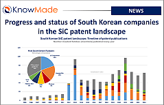
Featured image of the article Progress and status of South Korean companies in the SiC patent landscape.
SOPHIA ANTIPOLIS, France – 27 May 2025 │ Previous patent analyses conducted in 2022 have confirmed the emergence of a domestic SiC industry in South [...]
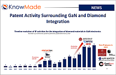
Featured image of the article Patent Activity Surrounding GaN and Diamond Integration.
SOPHIA ANTIPOLIS, France – July 30, 2024 │ GaN electronic devices, especially GaN-based high electron mobility transistors (HEMT), are increasingly used in RF and power [...]

June 19, 2025

Webinar – Navigating 2024’s Silicon Carbide Patent Landscape: Key IP Trends & IP Players

SOPHIA ANTIPOLIS, France – June 17, 2025 │Dr. Rémi Comyn discusses the entire intellectual property battle surrounding SiC technology in 2024 in a free webinar. Gain a comprehensive and in-depth overview of the competitive landscape and innovation. PDF and video available.

Webinar video recording


About the subject

This webinar delivers a deep dive into the 2024 intellectual property (IP) landscape across the Silicon Carbide (SiC) power device supply chain. We begin by quantifying overall patenting activity, spotlighting the leading corporate assignees—such as Wolfspeed, Infineon, Onsemi, and STMicroelectronics—and examining how their strategic patent filings reveal competitive positioning in substrates, epitaxial processes, device architectures, and packaging solutions. Next, we analyze the remarkable acceleration of SiC patent applications originating from China, exploring its drivers, key domestic players, and potential impacts on global IP competition. Finally, we synthesize recent patent filings to uncover emerging technological trajectories—ranging from engineered SiC substrates to next-generation SiC devices and advanced packaging solutions—that are poised to shape the evolution of SiC power electronics.

Webinar presentation slides

About the author

Rémi Comyn works for KnowMade as a Senior Patent Analyst in the field of Compound Semiconductors and Electronics. He holds a PhD in Physics from the University of Nice Sophia Antipolis (France) in partnership with CRHEA-CNRS (Sophia Antipolis, France) and the University of Sherbrooke (Québec, Canada). Rémi previously worked in compound semiconductors research laboratory as Research Engineer.

May 27, 2025

Progress and status of South Korean companies in the SiC patent landscape

SOPHIA ANTIPOLIS, France – 27 May 2025 │ Previous patent analyses conducted in 2022 have confirmed the emergence of a domestic SiC industry in South Korea. Driven by government-sponsored national programs, South Korean material conglomerates SK group (including SKC, SK Siltron, SK Inc., SK Innovation), Posco and LG group (including LG Chem, LG Electronics and its subsidiary LG Innotek) have built large patent portfolios. Their intellectual property (IP) activity has focused on unlocking SiC substrate technology and thereby addressed a potential bottleneck of SiC technology. As a result, South Korea has laid solid foundation for its future domestic SiC industry. Meanwhile, Hyundai Motor took the IP leadership over the research organization KERI (Korea Electrotechnology Research Institute) in developing SiC power devices, especially for electric vehicle (EV) applications.

Over the last decade, notable South Korean players from the national academic scene as well as from the local semiconductor industry have started SiC developments, entering the IP landscape and contributing to the consolidation of an emerging domestic SiC supply chain.

In late 2022, SK Inc. acquired Yes Powertechnix (now SK Powertech) – then the only South Korean firm able to design and produce SiC power management ICs. By leveraging synergies with other subsidiaries (SK Siltron, SK Hynix, etc.), SK group would have the potential to compete with leading SiC integrated device manufacturers (IDM) such as Wolfspeed, STMicroelectronics, Rohm Semiconductor, Infineon and onsemi.

Combining patent data from its SiC monitoring service with recent analyses from its latest SiC IP report, KnowMade has investigated the progress of the South Korean SiC industry from a patent perspective since 2022:

  • What is the current IP status of the main South Korean IP players?
  • Does any single company control IP across the entire SiC supply chain?
  • What has been the trajectory of 2010’s new entrants?
  • Who are the latest IP newcomers and where do they stand in the supply chain?

Six companies accounting for 66% of all South Korean inventions in the SiC patent landscape

Koreans’ patenting activity surged in the 2010s, peaking in 2021 with strong contributions from SKC, LG Chem and Hyundai Mobis (Figure 1). In 2022, the number of inventions disclosed by South Korean IP players slumped, in a context of fast growth for EV, the main application driving the SiC power device market. The year seems to mark a reorganization of SiC activities among most South Korean industrial players, with SKC spinning off a SiC substrate company (Senic), LG Innotek selling key SiC patents (LX Semicon, S-tech) and SK Inc. acquiring Yes Powertechnix (YPT). Concomitantly, several material companies drastically reduced their IP activity (Posco, LG group and SK group).

Furthermore, the first signs of an expansion of IP activities into SiC devices and downward the SiC supply chain (e.g., SiC packaging) by main IP players (LG group, SK group) were not confirmed by new patent filings in these areas after 2021. A year later, Hyundai Motor started following the same trend, exhibiting a steady reduction in the number of new inventions.

Yet the IP activity in the South Korean SiC patent landscape has remained robust since 2022. This dynamism is due to the entry of many IP newcomers in the field of SiC substrates (10+), SiC devices (5) and SiC circuits (20+). As a result, a plateau is observed in the number of inventions disclosed between 2022 and 2024 (Figure 1).

Bar graph showing the timeline of patent publications by South Korean players in the power SiC patent landscape.

Figure 1: Timeline of patent publications by South Korean players in the power SiC patent landscape and total percentage of inventions disclosed by main South Korean IP players for SiC technology.

SiC power modules: the weak link in the South Korean SiC supply chain?

Figure 2 describes the position of main South Korean IP players across the SiC supply chain, based on the number of inventions disclosed in each segment (bulk and bare wafer, epitaxial substrates, etc.). Hyundai dominates the downward supply chain while LG group leads in the upward segments. Accordingly, no single South Korean company is currently able of controlling IP over the whole supply chain.

Although South Korean main IP players together appear to cover the whole SiC supply chain, power modules seem to remain the weakest link. Indeed, the number of inventions related to SiC packaging and SiC power modules has not progressed significantly since 2022. This stagnation reflects the limited number of firms involved in this activity (Hyundai Motor, Amosense, JMJ Korea) and the reduced number of IP new entrants since 2022 compared to the other segments of the SiC supply chain (SemiPowerex).

Spun-off from SKC in 2021, Senic has made a remarkable entry in the South Korean SiC landscape, becoming rapidly one of the main IP players for SiC substrates (Figure 2). What’s more, the startup company has rapidly moved from the status of IP challenger to the status of IP leader in this segment of the SiC supply chain (Figure 3). Filing patent applications in most of the strategic countries for the semiconductor industry, the spin-off confirms its ambition to address the global SiC substrate market in coming years.

In contrast, LX Semicon, which acquired in 2021 IP rights on more than 20 inventions related to SiC epitaxial substrates and assigned to LG Innotek, did not seek to expand its IP leadership in recent years. Instead, the company announced in June 2024 its intention to downsize its R&D operations for SiC technology, signaling a potential exit from the SiC industry.

In the SiC device patent landscape, EYEQ Lab, which entered the IP space in 2020 and is reportedly expanding from fabless design to foundry services, published four additional domestic patent applications in 2023, focusing on dicing methods and wire-bond interconnects for SiC Schottky diodes.

Arrow graph showing each step of the South Korean SiC supply chain from a patent perspective.

Figure 2: Mapping of main patent assignees and most recent IP newcomers across the SiC supply chain based on their patent filings.

Hyundai Motor and Senic expanding their IP leadership outside South Korea

The main IP trends discussed previously can be summarized by Figure 3. The IP leadership graph compares the IP position of main IP players between 2021 and 2024 in the SiC patent landscape. Accordingly, Hyundai Motor has confirmed its IP leadership for SiC power devices while Senic now leads in SiC boules and bare wafers. Furthermore, SK group has also improved its IP position in the last three years, focusing on SiC substrates (including SiC boules, bare and epitaxial wafers).

In contrast, LG group shifted its IP position from being IP leader in 2021 to a well-established player holding a high number of granted patents but exhibiting a much-reduced patenting activity in 2024. Furthermore, Posco and KERI’s IP positions have not changed significantly in their respective fields, with IP activities largely confined to domestic filings.

Bubble graph showing the IP leadership of South Korean companies in SiC patent landscape.

Figure 3: IP leadership of South Korean patent assignees in the power SiC patent landscape.

TRinno Technology and EtaMax just joined the SiC IP competition

The main South Korean IP newcomer since 2021 has been TRinno Technology, which published its first SiC-related patents in 2022. The power semiconductor company filed 7 patent families (inventions), covering both planar and trench SiC MOSFET technologies. Interestingly, all patent families have already been granted in South Korea. However, TRinno Technology is also seeking protection of 4 inventions abroad, in China, USA and Europe.

Another notable IP newcomer is EtaMax which entered the SiC substrate patent landscape in 2022, focusing on defect identification and die division, to minimize the influence of a wafer defect on the final semiconductor chip. EtaMax is assigned to several SiC patent applications in the US.

Are Samsung and DB Hitek re-entering the SiC (IP) arena?

Several major South Korean semiconductor companies in the global semiconductor landscape have announced plans to enter the SiC semiconductor market. These include Samsung Electronics which has had a limiting patenting activity in the SiC device patent landscape so far. Its most recent patent application was published in 2023 and describes a gate trench SiC MOSFET structure having source trenches and a pair of shielding regions.

Likewise, DB Hitek resumed its patenting activity last year after a 15-years break in the SiC patent landscape.  The South Korean foundry disclosed three inventions describing both planar and trench gate MOSFET designs, including a planar SiC MOSFET integrated with a SiC Schottky diode.

Eventually, KEC, a power semiconductor company with capabilities to design and produce SiC power devices, resumed its patenting activities in 2024, after its last patent filings in 2017. Four domestic patent applications have been filed in South Korea, covering SiC trench Schottky diodes, SiC planar MOSFET and SiC trench MOSFET.

KnowMade’s Value Proposition

The present case study illustrates the complementarity of KnowMade’s solutions to get access to the most comprehensive picture of the SiC competitive IP landscape at any time. The monitoring service allows to track in real-time the patenting activity of key players in the semiconductor industry, regardless of their level of patenting activity in the SiC patent landscape and whatever is their position in the SiC supply chain. On the other hand, the IP report provides in-depth patent analyses of global IP trends. Together, they empower customers to capture the big picture across 20,000+ patents and to detect emerging, high-value signals from even the smallest pool of filings.


Press contact
contact@knowmade.fr
Le Drakkar, 2405 route des Dolines, 06560 Valbonne Sophia Antipolis, France
www.knowmade.com

About the author
Rémi Comyn, PhD. Rémi works at KnowMade as Senior Analyst in the field of Compound Semiconductors and Electronics. He holds a PhD in Physics from the University of Nice Sophia-Antipolis (France) in partnership with CRHEA-CNRS (Sophia-Antipolis, France) and the University of Sherbrooke (Québec, Canada). Rémi previously worked in compound semiconductors research laboratory as Research Engineer.

About KnowMade
KnowMade is a Technology Intelligence and IP Strategy consulting company specialized in analysis of patents and scientific information. The company helps innovative companies and R&D organizations to understand their competitive landscape, follow technology trends, and find out opportunities and threats in terms of technology and patents.
KnowMade’s analysts combine their strong technology expertise and in-depth knowledge of patents with powerful analytics tools and methodologies to turn patents and scientific information into business-oriented report for decision makers working in R&D, Innovation Strategy, Intellectual Property, and Marketing. Our experts provide prior art search, patent landscape analysis, scientific literature analysis, patent valuation, IP due diligence and freedom-to-operate analysis. In parallel the company proposes litigation/licensing support, technology scouting and IP/technology watch service.
KnowMade has a solid expertise in Compound Semiconductors, Power Electronics, Batteries, RF Technologies & Wireless Communications, Solid-State Lighting & Display, Photonics, Memories, MEMS & Solid-State Sensors/Actuators, Semiconductor Manufacturing, Packaging & Assembly, Medical Devices, Medical Imaging, Microfluidics, Biotechnology, Pharmaceutics, and Agri-Food.

July 30, 2024

Patent Activity Surrounding GaN and Diamond Integration

SOPHIA ANTIPOLIS, France – July 30, 2024 │ GaN electronic devices, especially GaN-based high electron mobility transistors (HEMT), are increasingly used in RF and power conversion applications. Yet in the most demanding applications, GaN device performance and reliability may be limited by thermal considerations such as the channel temperature. Some forms of enriched monocrystalline synthetic diamond have been shown to have the highest thermal conductivity of any known solid at room temperature 1. Because of this thermal conductivity, the integration of diamond into GaN electronic structures can significantly improve the thermal management of GaN devices. However, such integration has been technically challenging so far. In its latest GaN electronics reports, KnowMade highlights endeavors to leverage GaN with diamond integration in electronic devices based on the recent patent applications filed in this space.

This analysis was previously published in the June 2024 print edition of the Microwave Journal.

Many IP newcomers enter the field

The patent analysis is broad. It considers all patent applications claiming the integration of diamond with GaN electronics without distinction of the material, so it includes applications using single-crystal diamond, polycrystalline diamond and other varieties. The analysis does not differentiate as to the stage of the process where the diamond was integrated. This integration can be a passivation layer, a substrate, a heat sink or another use. It also does not distinguish whether the diamond was integrated as epitaxy, bonding or in some other fashion.

With these guidelines, Figure 1 describes the time evolution of intellectual property (IP) activities related to the technical challenge of integrating diamond materials with GaN. As Figure 1 shows, patenting activities were very limited in the 2000s, but they took off in the early 2010s. The driving forces behind the increase in patent activity were the efforts of pioneers such as Element Six and Group4 Labs.

Founded in 2003 as a U.S. startup company, Group4 partnered with Element Six in 2008. Group4 was subsequently acquired by Element Six in 2013. In 2016, newly established Akash Systems agreed with RFHIC to jointly negotiate the repurchase of Element Six’s GaN-on-diamond IP. Akash acquired all patents and other IP rights related to GaN-on-diamond technology for use in satellite communications and related markets.

Table showing the timeline evolution of IP Activities for the integration of diamond materials in GaN electronics.

Figure 1: Time evolution of patent family publications for the integration of diamond materials with GaN electronic devices.

In 2021, the number of patent filings increased sharply, mainly due to the acceleration of Chinese players such as CETC with 29 inventions and Xidian University with 44 inventions. Since 2021, a relatively stable patenting activity has been observed, supported by the entrance of more than 30 new IP players, especially Chinese research organizations like Wuhan University, Shenzhen University and Taiyuan University of Technology, along with Chinese industrial players like CoolSemi, CSMH and others.

Besides China, several players like Air Water in Japan, which collaborated with Osaka Metropolitan University, have entered the field recently. This collaboration co-filed patent WO2023/048160, published in early 2023. The patent publication was followed by a scientific paper released in late 2023 2. In this paper, researchers described a method based on the heteroepitaxy of GaN on a 3C-SiC layer formed on a silicon substrate. Then, the silicon substrate is removed and the GaN-on-3C-SiC stack is bonded to a thermally conductive support layer that can be made of either diamond or polySiC, according to the first patent claim. So far, about 30 patent families have disclosed methods based on bonding techniques to integrate diamond materials with GaN electronic devices.

However, bonding of GaN materials with a diamond substrate is technically challenging and alternative methods have been developed. For instance, Wonder CVD, a startup company founded in 2016 and headquartered in Dubai, entered the GaN electronics patent landscape in 2023, filing patent application US20230307249. It describes the growth of polydiamond on the silicon (111) thin layer of an SOI substrate, the removal of the base and oxide layers, followed by the heteroepitaxy of GaN on the other surface of the silicon (111) thin layer.

Another interesting example is the collaboration between imec and UHasselt in Europe that is described in patent EP4125113, although the patent application seems to have been abandoned since August 2023. The invention relates to the formation of a nanocrystalline diamond layer that forms a stable connection between a GaN material and a polydiamond material. In addition, the nanocrystalline diamond layer is expected to further facilitate heat dissipation for GaN electronic devices.

While the previous examples describe the integration of diamond materials in contact with or relatively close to the GaN device layer, US startup company Diamond Foundry entered the GaN electronics patent landscape in 2023 with a different approach. In patent application US20230411459, Diamond Foundry disclosed a diamond substrate that could be used as a packaging substrate for GaN or SiC devices intended as an alternative to silicon-based IGBT chips used in electric vehicle applications. Diamond Foundry is one of the few companies in this space targeting power applications. Overall, less than 10 percent of all inventions related to diamond integration explicitly target power electronics. Figure 2 shows a drawing from US20230411459 illustrating Diamond Foundry’s idea for their diamond substrate.

Illustration of diamond materials intergation in power electronics.

Figure 2: Patent application US20230411459, assigned to Diamond Foundry: A novel single-crystal diamond wafer enables significant advances in electric vehicle power electronics.

The IP Leaders

Comparing the number of pending patent applications with the number of granted patents for the main patent assignees provides valuable insight into the global IP competition for a given technology. Figure 3 shows this comparison for the integration of diamond materials with GaN electronics. Figure 3 plots the number of pending patent applications on the x-axis and the number of granted patents on the y-axis. At this intersection of these metrics, the size of the bubble represents the number of patent families selected for the study. The results of Figure 3 show that RFHIC stands as the current leader in GaN and diamond-related IP, but several RF GaN market players have positioned themselves as challengers. As can be seen, Akash Systems is the closest competitor to RFHIC, trailing slightly in patent applications and patents granted. However, companies like RTX Corporation, Mitsubishi Electric, Xidian University and CETC could pose strong future competition as all of them have more patent applications than RFHIC. Additionally, Mitsubishi Electric, Xidian University and CETC have comparable or much more breadth of GaN and diamond-related patent families. RFHIC’s current IP leadership is largely inherited from the patenting activities of Group4 and Element Six, although a few inventions were disclosed by RFHIC soon after the patent transaction, in 2018.

Graphic showing IP leadership in the sector of diamond integration in GaN electronics.

Figure 3: IP leadership of patent assignees filing patents related to the integration of diamond materials into GaN electronic devices.

In its 2023 GaN electronics IP report, KnowMade analyzed this IP leadership and pointed out RFHIC’s IP strength in GaN-on-diamond wafers and epiwafers, which is the very upward part of the RF GaN supply chain. In this part of the supply chain, RFHIC has no serious IP challengers but Xidian University. Because most of its patents are recent and exclusively filed in China, Xidian University’s IP leadership remains limited despite a relatively high number of inventions disclosed by the Chinese university. In contrast, RFHIC’s patent portfolio protects inventions in many different countries, especially in Europe, Japan, the U.S. and South Korea.

Details from 6 patents related to Gan/diamond.wafers

Figure 4: US patents related to GaN/diamond wafers recently granted to RFHIC.

Interestingly, RFHIC resumed its patenting activities in 2021 with the publication of seven new inventions related to GaN-on-diamond. At the same time, they confirmed a global IP strategy, especially for one invention protected by several foreign patents, including six U.S. patents. The invention relates to the transfer of a III-nitride layer from its silicon growth substrate to a support wafer via a diamond layer. Different aspects of the method have been protected through various patent applications. For instance, an intermediate layer between the III-nitride layer and the diamond layer (US11652146), a composite silicon/diamond support wafer (US11652146) and the deposition of the support wafer (e.g., with polyGaN or polysilicon in US11476335), the carrier wafer (e.g., a SiC carrier is mentioned in US11424328) and the formation of through holes in such engineered substrates, as described in patent applications US11901418 and US11901417. Drawings from these and other patents granted to RFHIC for GaN/diamond wafers are shown in Figure 4.

Just like RFHIC, U.S. company Akash Systems published only a few inventions after the patent acquisition from Element Six. Akash published two patent families in 2018, mentioning the integration of diamond at the device level as a substrate and package level as a base for improved thermal management in transmitters used in satellite communication (US10332820, US10374553). Interestingly, the U.S. startup company resumed its IP activities in 2020, publishing seven inventions aiming to increase its coverage of the RF GaN supply chain. These recent inventions relate not only to packages, modules and systems but also to wafers, epiwafers and devices.

Mitsubishi Electric started its patenting efforts in 2017 and has maintained a stable IP activity in the field. In contrast with other competitors aiming to protect inventions across the entire supply chain, Mitsubishi Electric’s IP strategy seems to focus on developing various aspects related to GaN-on-diamond device technology. Starting from an epiwafer, GaN layer transfer (US20230083507) and GaN bonding (US20220230920) techniques have been disclosed to integrate GaN devices with a diamond substrate. In an alternative approach, diamond may be integrated locally below the GaN devices with good adhesion characteristics and limited damage to the GaN epilayer. This concept is shown in Figure 5 with a drawing from US10720374 granted to Mitsubishi Electric in 2020. Additionally, the company has several patents related to the fabrication of GaN devices on recessed diamond substrates (e.g., US11482464).

Scheme of the result of layering diamond on nitride.

Figure 5: Formation of a diamond layer on a nitride layer (Mitsubishi Electric, US10720374, granted in 2020).

Conclusion

IP activities related to the integration of diamond materials into GaN electronics devices have remained marginal in the GaN electronics patent landscape. For comparison, these activities represent less than 10 percent of all inventions related to RF GaN disclosed in 2023. Yet the analysis of the IP competition highlights a significant activity in recent years from several market players, in terms of the number of inventions disclosed by these players and the volume of patent applications filed to protect some of their key inventions in multiple countries. Additionally, since there is a limited number of well-established players in this space, there seems to be an opportunity for newcomers to make a breakthrough in this landscape, not only in terms of technology but also in terms of IP.

References

[1]

en.wikipedia.org/wiki/Material_properties_of_diamond#Thermal_conductivity

[2]

onlinelibrary.wiley.com/doi/10.1002/smll.202305574


Press contact
contact@knowmade.fr
Le Drakkar, 2405 route des Dolines, 06560 Valbonne Sophia Antipolis, France
www.knowmade.com

About the author
Rémi Comyn works for KnowMade as a Patent Analyst in the field of Compound Semiconductors and Electronics. He holds a PhD in Physics from the University of Nice Sophia Antipolis (France) in partnership with CRHEA-CNRS (Sophia Antipolis, France) and the University of Sherbrooke (Québec, Canada). Rémi previously worked in compound semiconductors research laboratory as Research Engineer.

About KnowMade
KnowMade is a Technology Intelligence and IP Strategy consulting company specialized in analysis of patents and scientific information. The company helps innovative companies and R&D organizations to understand their competitive landscape, follow technology trends, and find out opportunities and threats in terms of technology and patents.
KnowMade’s analysts combine their strong technology expertise and in-depth knowledge of patents with powerful analytics tools and methodologies to turn patents and scientific information into business-oriented report for decision makers working in R&D, Innovation Strategy, Intellectual Property, and Marketing. Our experts provide prior art search, patent landscape analysis, scientific literature analysis, patent valuation, IP due diligence and freedom-to-operate analysis. In parallel the company proposes litigation/licensing support, technology scouting and IP/technology watch service.
KnowMade has a solid expertise in Compound Semiconductors, Power Electronics, Batteries, RF Technologies & Wireless Communications, Solid-State Lighting & Display, Photonics, Memories, MEMS & Solid-State Sensors/Actuators, Semiconductor Manufacturing, Packaging & Assembly, Medical Devices, Medical Imaging, Microfluidics, Biotechnology, Pharmaceutics, and Agri-Food.