SOPHIA ANTIPOLIS, France – September 06, 2024 │Propelled by the increasing demand for data processing in high-performance computing (HPC) applications, 5G and beyond communication networks, and autonomous vehicles, a tremendous number of new inventions related to advanced semiconductor packaging have been published in recent years. By analyzing patents, the technological evolutions and the competitive landscape can be monitored. In this overview, we shed light on the growing patenting activity related to fan-out packaging, interposers and interconnect bridges, and hybrid bonding. While historical players have expanded their patent portfolios, new entrants have recently joined the intellectual property (IP) landscape with a blooming patenting activity.
IP dynamics of advanced semiconductor packaging technologies over the years
For many years, wire-bond and flip-chip technologies have been at the forefront of traditional semiconductor packaging innovations. With the rising demand for scaling and thereby combining more chips inside the same package to process massive quantities of data, the IP landscape has diversified with advanced semiconductor packaging segments like fan-out and 2.5D/3D IC packaging technologies. The diversity and co-developments of semiconductor packaging technologies make the patent landscape more complex (Figure 1). Fan-out wafer-level packaging (WLP) related patent publications gained momentum in the 2010s and continues to increase. Indeed, by spreading the I/O out further in a reconstituted wafer (or panel) and connecting chips to a redistribution layer (RDL), fan-out WLP enables higher I/O density. Advanced interconnects implemented to connect the packaged dies side by side or on top of each have also been the subject of many new inventions in recent years. In 2.5 D packaging, patent publications related to interposers and bridge interconnects have been increasing steadily, with the bridge segment seeing a recent acceleration. In 3D packaging, the well-established microbump technology faces limitations in achieving fine pitches below 10 micrometers, expanding I/O, increasing bandwidth, heightening power efficiency, and reducing parasitics and thermal resistance. In this context, hybrid bonding has become a key packaging technology and is gaining more IP interest. This method combines dielectric-to-dielectric and metal-to-metal bonds to interconnect wafer-to-wafer, die-to-wafer, or die-to-die without the need for solder or other adhesives.
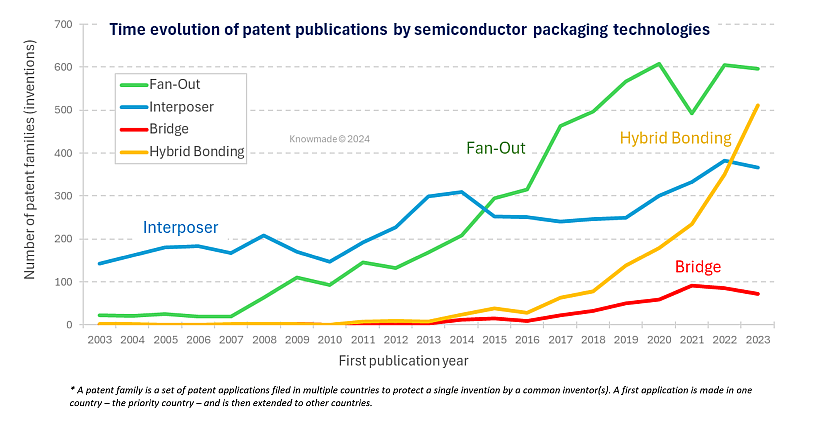
Figure 1: Time evolution of patent publications related to fan-out packaging, interposers, embedded bridge interconnects, and hybrid bonding.
Fan-out packaging
Since 2016, KnowMade has been tracking the IP evolution related to fan-out packaging, including multi-chip 2.5D/3D fan-out wafer level and panel level, and fan-out package-on-package. From the beginning, the early innovators came from a broad range of typologies, including foundries like TSMC, semiconductor companies such as Infineon, NXP/Freescale, Samsung, and Intel, and OSATs like ASE, SPIL, JCET/STATS ChipPAC, and Amkor/J-Devices/Nanium. Over the last 10 years, the patent filings have continued at a rapid pace, with new patent applicants joining the IP landscape, such as TongFu (OSAT), SJSemi (SMIC/JCET joint venture), and materials suppliers like TOK, Resonac, Lintec, and HD Microsystems (Figure 2). These materials companies have conducted R&D efforts to meet the growing demand for innovative materials and processes, which are key to a successful fan-out process (molding materials, adhesives, lithographic resins, laminates). In recent years, the most active IP newcomers in the fan-out patent landscape are based in China, including Fozhixin Microelectronics (equipment supplier), Forehope Electronic (OSAT), Microsilicon Technology (OSAT), and NEXGO (which acquired all fan-out patents from NXP in 2019). Looking at the current IP landscape overall, TSMC is clearly leading the Fan-Out IP competition with the largest established patent portfolio and is continuing to file new patent applications, which will further enhance its IP portfolio in the coming years (Figure 3). TSMC’s Integrated Fan-Out (InFO) technology (e.g., US10340206) known for having equipped several iPhone models from Apple, leverages fan-out to extend its possibilities by integrating molded chips with high-density redistribution layer (RDL) and through InFO via (TIV) for high-density interconnect. Despite an unclear position in Fan-Out market until 2015, Samsung has been present in the Fan-Out patent landscape since mid-2000s and has significantly increased its patenting activity since 2015. After losing the Apple A10 manufacturing market in 2016 due to a lack of improvement in their packaging compared to TSMC, Samsung announced they will staff packaging project and launch a solution to compete with TSMC’s InFO. Today, Samsung is better positioned to challenge TSMC’s IP leadership.
In recent years, assembly and testing facilities (OSATs) have been actively promoting Fan-Out Panel Level Packaging (FOPLP) solutions, which offer advantages such as lower unit costs and larger package sizes. FOPLP technology has gained the attention of most IP players, and today, the main patent owners are Samsung, Fozhixin Microelectronics, Silicon Pan Microelectronics, Amkor and TongFu. FOPLP ecosystem is developing, while the leading semiconductor foundry TSMC appears to be forming a team and establishing a mini line to develop FOPLP technology (source: TrendForce). The move to transition Fan-Out packaging from wafer level to panel level is becoming a reality.
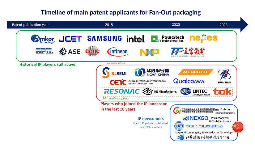
Figure 2: Timeline of main patent applicants for fan-out packaging.
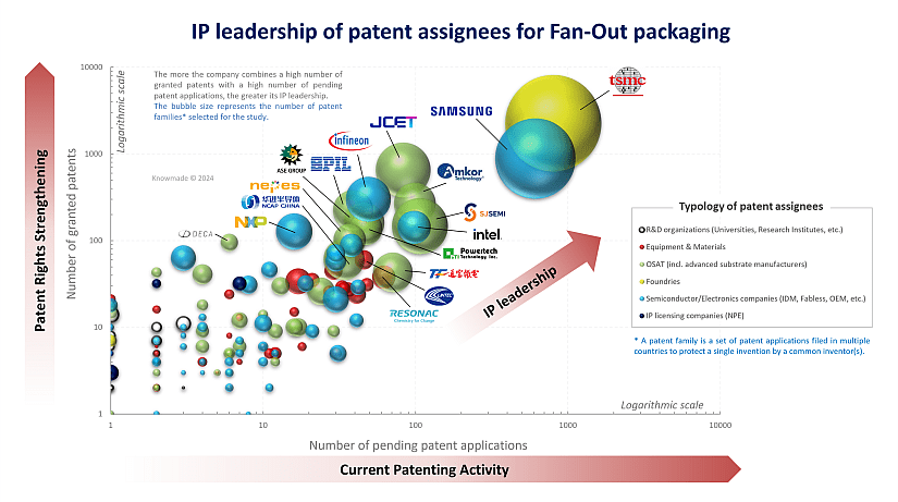
Figure 3: IP leadership of patent assignees for fan-out packaging.
Interposers and bridge interconnects
Interposers (silicon, glass, or organic substrates placed between dies and PCB or between multiple dies) facilitate connections, enable higher I/O density, and improve performance. Bridge interconnects (small pieces that enable direct die-to-die connections) allow for efficient communication between multiple chips, minimizing latency and power consumption while improving signal integrity. The patent activity related to 2.5D interposers has been gaining momentum since the early 2010s and is continuously growing, especially with the developments of TSMC’s CoWoS®, Intel’s Foveros and Samsung’s I-Cube™ & H-Cube™ technologies. In the first decade, bridge-related IP landscape was driven mostly by Intel with the development of its Embedded Multi-die Interconnect Bridge (EMIB) technology, later joined other patent applicants such as TSMC, Samsung, IBM, SK Hynix, AMD, JCET, and SJSemi. Advantageously, bridges and interposers can be combined inside the same package, like in Intel’s EMIB 3.5D, that combines Forveros and EMIB. This versatility offers extended possibilities for heterogenous integration and new patent filings can be expected. Intel is developing glass core interposers (US20230187331) with through glass vias (TGVs) and openings to include one or more die. Other Intel’s recent inventions points at the use of glass core material to fabricate the bridge die and achieve high-speed I/O (US20230317618, US20220384330). Indeed, traditional silicon-based bridges are relatively expensive and may have a longer process flow than desired. ASE is continuing R&D efforts on its FOCoS technology featuring a silicon bridge die embedded in a fan-out RDL, aiming at solving challenges in the manufacturing process (CN218887191, CN218827084, CN219642825, CN219937049). Structure engineering and materials integration possibilities enhance 2.5D advanced packaging capabilities and the interposer/bridge IP segment is thriving. TSMC, Samsung and Intel are leading this interposer/bridge patent landscape, and their IP position will strengthen as they are ahead of other patent applicants by considering the number of new patent applications.
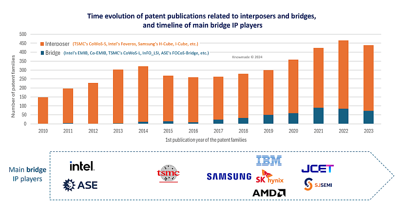
Figure 4: Time evolution of patent publications related to interposers and bridges, and timeline of main bridge IP players.
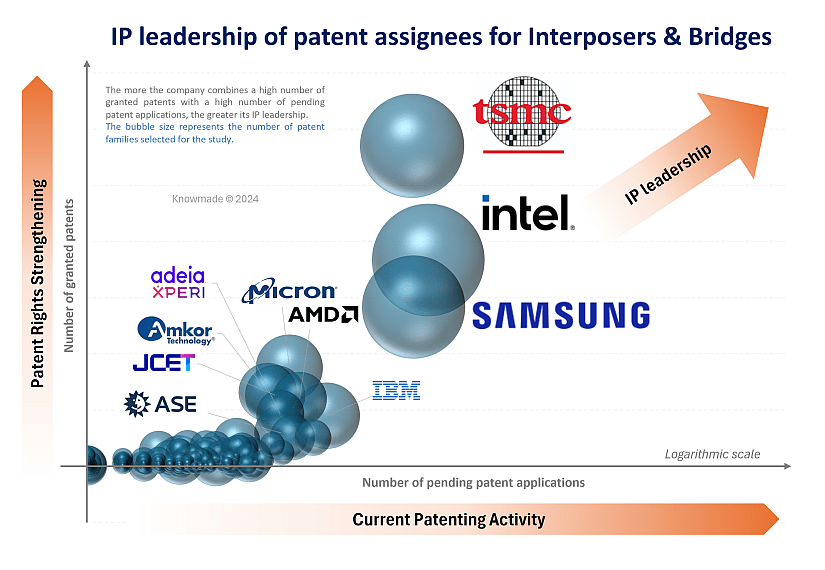
Figure 5: IP leadership of patent assignees for interposers & bridges.
Hybrid bonding
Hybrid bonding is used for the vertical stacking of multiple chips, enabling 3D heterogeneous integration and interoperability of different types of chips with various functions (e.g., logic, memory, analog, sensors) within a single package. By implementing direct metal-to-metal and oxide-to-oxide connections without the use of solder balls or other adhesives, hybrid bonding technology enables finer pitches (<10µm, or even <1µm) with significant benefits for interconnect density and device performance. In addition, this bonding technology facilitates efficient heat dissipation, reduces parasitic delay, and avoids signal interference between metal pads.
Over the past five years, hybrid bonding technology has become a key enabler of advanced packaging and is now being adopted across the semiconductor industry for various applications, including memory, logic, RF, and photonics. As pioneer and owner of the direct bond interconnect (DBI) technology of Ziptronix acquired in 2015, Adeia (formerly Xperi) has adopted an aggressive strategy to assert its patents and license its hybrid bonding IP portfolio to various semiconductor companies (Sony, YMTC, Micron, Kioxia, etc.). Despite Adeia/Xperi’s historically strong IP position, other players have been developing their own patent portfolios related to hybrid bonding processes or die stacking using hybrid bonding technology. Since the early days, both TSMC and Intel invested in R&D efforts to harness this cutting-edge bonding technology, ultimately resulting in advanced packaging technologies for chiplets, such as TSMC‘s 3D-stacked system-on-integrated chips (SoIC) and Intel’s Foveros Direct 3D and EMIB 3.5D (i.e., a combination of EMIB and Foveros). More players are eager to use hybrid bonding technology or sell products utilizing it, and they are moving fast thanks to the development of their IP portfolios and license offerings from Adeia. YMTC and Samsung hold Adeia’s licenses and have also been investing in R&D and developing their own hybrid bonding patent portfolios to support their respective 3D IC technologies, Xtacking® and X-Cube™.
Since 2019 and the release of our first Hybrid Bonding IP report, the number of related patents has increased more than fourfold, and the patent landscape has evolved. Major patent owners have strengthened their IP positions, reinforcing the geographical protection of their inventions in the US, China, and Europe, while various new patent applicants have entered the patent landscape. These IP trends attest that hybrid bonding is becoming a business reality.
In our new Hybrid Bonding patent landscape report, we update the analysis of IP and technology trends and highlight the patent activities of main players and newcomers.
TSMC is still leading the Hybrid Bonding patent landscape from a quantitative viewpoint, with most inventions related to hybrid-bonded semiconductor structures or devices, mainly focused on 2.5D/3D IC applications (e.g. US20230335519). YMTC and Adeia have significantly increased their enforceable patent portfolios in recent years. Adeia’s IP portfolio is well balanced between inventions related to the hybrid bonding process and interface engineering and inventions on hybrid-bonded semiconductor structures or devices. Adeia owns the highest number of key patents related to the bonding process itself, thus the IP portfolio contains a wide variety of innovations to improve the reliability of the hybrid bonding structures (thermal management US11011494, mechanical stress US11296053, metal diffusion US11031285, bonding strength US20230197453, etc.). YMTC’s hybrid bonding patents stand out for 3D-stacked memory (e.g. US11037945). Whereas before 2020, foundries and device makers were involved in the IP race, OSATs and equipment/materials suppliers have recently joined the patent landscape with flourishing IP portfolios and now appear as new IP challengers (ASE, SJSemi, TongFu, Applied Materials, Resonac).
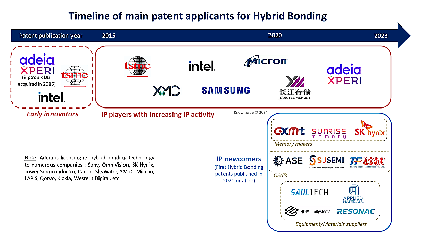
Figure 6: Timeline of main patent applicants for hybrid bonding.
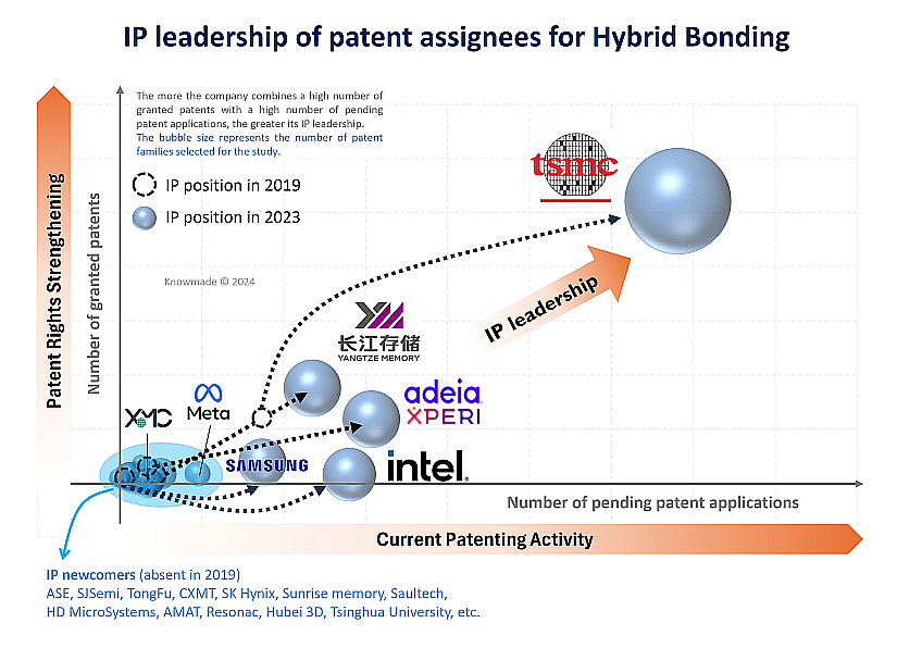
Figure 7: IP leadership of patent assignees for hybrid bonding.
China’s capability in the advanced semiconductor packaging sector
US restrictions on China’s access to advanced chips and foundry technologies have driven Chinese efforts to achieve semiconductor self-sufficiency, accelerating the development of a domestic semiconductor industry. The local ecosystem relies on companies such as YMTC and CXMT for memory chip production, SMIC and XMC for foundry services, and JCET, Huatian Technology, TongFu Microelectronics, SJSemi and NCAP for testing, assembly, and packaging services. As an alternative to using the most advanced node technologies to produce leading-edge semiconductor devices, China is developing its advanced packaging technologies.
In recent years, Chinese companies have significantly invested in developing their own intellectual property (IP) related to advanced semiconductor packaging. In the field of Fan-Out packaging, JCET, SJSemi, TongFu, and NCAP are currently well-positioned to challenge the IP leadership of TSMC and Samsung (Figure 3). Moreover, most of the new entrants in the IP landscape are Chinese (Figure 2). In hybrid bonding technology, YMTC and XMC are increasing their patenting activity, and newcomers like SJSemi, CXMT, and TongFu have made a noticeable entry into the IP landscape over the last 3 years. Finally, the multi-die interconnect bridge technology is also being invested by Chinese patent applicants such as SJSemi (CN114937608, CN115148611) and JCET (CN116598291).
Patent analysis indicates that Chinese players possess the capabilities to circumvent US restrictions on chip development through their advanced semiconductor packaging technologies and related IP. They are now on the verge of challenging leading companies in Taiwan, the US, and South Korea. Soon, they may be able to enforce their advanced packaging-related patents and could target industry leaders in key market regions.
Press contact
contact@knowmade.fr
Le Drakkar, 2405 route des Dolines, 06560 Valbonne Sophia Antipolis, France
www.knowmade.com
About the author
Pauline Calka, PhD. works for KnowMade as a patent analyst in the fields of semiconductor manufacturing and advanced packaging. She holds a PhD in Memory from the University of Grenoble Alpes (France), in partnership with the CEA-Leti (France). After an Alexander von Humboldt Postdoc fellowship position at the Technical University of Berlin (Germany) and the Leibniz Institute for High Performance Microelectronics on ReRAM development, Pauline worked five years at ASM International (Belgium) as Senior Process Engineer on thin film development for logic, memory and MEMS, and two years at CEA-Leti as Integration Engineer on imaging CMOS sensors.
About KnowMade
KnowMade is a technology intelligence and IP strategy consulting company specialized in analyzing patents and scientific publications. The company helps innovative companies, investors, and R&D organizations to understand competitive landscape, follow technological evolutions, reduce uncertainties, and identify opportunities and risks in terms of technology and intellectual property.
KnowMade’s analysts combine their strong technology expertise and in-depth knowledge of patents with powerful analytics tools and methodologies to turn patent information and scientific literature into actionable insights, providing high added value reports for decision makers working in R&D, innovation strategy, intellectual property, and marketing. Our experts provide prior art search, patent landscape analysis, freedom-to-operate analysis, IP due diligence, and monitoring services.
KnowMade has a solid expertise in Compound Semiconductors, Power Electronics, Batteries, RF Technologies & Wireless Communications, Solid-State Lighting & Display, Photonics, Memories, MEMS & Sensors, Semiconductor Packaging, Medical Devices, Medical Imaging, Microfluidics, Biotechnology, Pharmaceutics, and Agri-Food.