SOPHIA ANTIPOLIS, France – April 07, 2025 │ Optical interposers are a crucial technology for advanced semiconductor packaging and co-packaged optics, driving the rapid growth of artificial intelligence (AI) and high-performance computing (HPC) applications by enabling data transmission through light rather than traditional electrical signaling. Several companies are actively developing optical interposers and related photonics. In addition to semiconductor companies, specialized firms are gaining prominence in the industry by expanding their Intellectual Property (IP) portfolios.
Optical Interposers: A Key Enabler for the Rapid Growth of AI Applications
An optical interposer differs from a standard silicon interposer by leveraging light for inter-chip data transmission instead of traditional electrical interconnects, making it highly suitable for applications that demand massive data movement with minimal power and latency overhead. Its key advantages include higher bandwidth for faster data transfer and reduced bottlenecks, lower power consumption by minimizing energy loss from resistance and capacitance, and improved efficiency. Additionally, optical signals travel faster with lower latency and minimal degradation over distance, enhancing system responsiveness. They also generate less heat than electrical interconnects, improving thermal management, and support long-distance communication with high signal integrity, making them ideal for scalable chiplet architectures. Thus, optical interposers have raised interest of the semiconductor industry.
Lightmatter Rises as a Leading Innovator in Photonics, Including Optical Interposers
Several companies are actively developing advanced photonics interconnect solutions and co-packaged optics. Key players include major semiconductor companies like Intel, Nvidia, Marvell, and Broadcom, and photonic interconnect & co-packaged optics specialized companies like Lightmatter, Ayar labs, and Ranovus.
Founded in 2017, Lightmatter raised $400 million in Series D funding in October 2024, reaching a $4.4 billion valuation and $850 million in total capital. The round included backing from investors such as T. Rowe Price Associates, Fidelity, and Google Ventures, to support the mass deployment of its Passage™ photonic engine, which uses 3D-stacked photonics. Besides, Lightmatter has been actively building a strategic patent portfolio, which reached more than 60 patent families as of March 2025 (Figure 1), in alignment with its technological roadmap and business growth. The increase in patent activity during key product development phases and funding milestones reflects a strong culture of innovation and a deliberate strategy to secure competitive advantages in the photonic computing space.
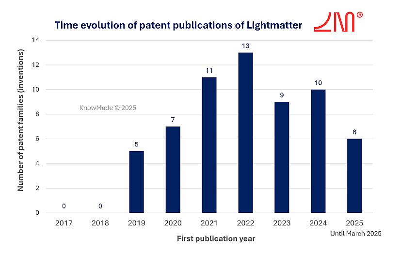
Figure 1: Time evolution of patent publications from Lightmatter.
Lightmatter’s Worldwide IP Coverage Reveals a Global Vision for Photonics
The American company has implemented a global IP strategy to protect its inventions (Figure 2). The U.S. remains its primary territory, demonstrating a strong presence with 59 granted patents and reinforcing it with 43 pending patent applications. In Taiwan, Japan, South Korea, China, and Europe, Lightmatter is building a significant IP portfolio with currently more than 120 pending patent applications, showing that it is gradually extending its territorial IP coverage. This IP strategy reflects that these regions are key strategic markets into which Lightmatter is aiming to expand. Overall, Lightmatter’s geographic IP coverage aligns with its ambition to become a global leader in the photonics market. In November 2024, the American company announced strategic partnerships with Advanced Semiconductor Engineering (ASE) and Amkor, two leading semiconductor packaging firms, to support the global deployment of its technology.
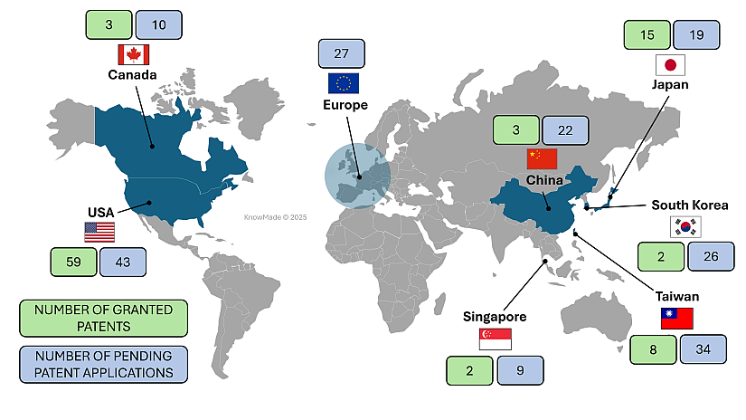
Figure 2: Geographical coverage of Lightmatter’s patent portfolio.
Lightmatter’s Patent Portfolio Overview
Lightmatter‘s patent portfolio primarily addresses critical bottlenecks in conventional electronic computing by leveraging photonics technology, utilizing optical signals to achieve high-speed, high-bandwidth, low-power computing and communication solutions. The patents collectively emphasize innovations in photonic computing architectures, integrated photonic packaging, analog-digital hybrid systems, and specialized neural network acceleration. Lightmatter‘s patent pools form a comprehensive portfolio constructed to address the computing needs of future data-intensive applications, particularly in AI and HPC.
Photonic Computing Systems & Processors
At least ten patents relate to photonic computing systems and processors, through which Lightmatter addresses the inherent limitations of conventional electronic processors, such as computational bottlenecks, power inefficiency, and latency constraints, particularly in demanding AI and deep-learning scenarios. Photonic computing solutions employ optical signals to perform high-speed matrix and tensor operations, vastly outperforming traditional digital architectures. Innovations include differential optical encoding, modulable detectors for compact integration, and optical encoders and multipliers enabling ultra-fast matrix-vector multiplications. These processors significantly accelerate complex computations, reducing operation times from nanoseconds to picoseconds, as exemplified by patents like US10763974 and US11700078.
Photonic Memory Integration & Communication Networks
Almost seven patents pertain to photonic memory integration and communication networks. A primary challenge addressed by Lightmatter’s photonic memory solutions is the bandwidth bottleneck and scalability limitations associated with conventional electrical interconnects. By integrating stacked memory layers with optical communication channels, the firm achieves unprecedented memory bandwidths exceeding 1 TB/s, significantly reducing power consumption and increasing physical scalability (US11367711). Programmable photonic networks further enhance flexibility, allowing dynamic and reconfigurable memory access, which facilitates efficient data transfer and system robustness through redundancy and fault-tolerance techniques, exemplified by patents like US11036002 and US12130484.
Photonic Packaging & Integration Technology
Almost ten patents are related to photonic packaging and integration technology, through which Lightmatter resolves the challenges of thermal management, electrical signal integrity, manufacturing complexity, and scalability in integrating electronic and photonic components. The company’s innovative interposer technologies, including programmable silicon and glass interposers, facilitate efficient electrical-photonic integration, significantly reducing inductance and parasitic impedance. Additionally, protective cavities and novel thermal management methods ensure reliability and performance stability, as seen in patents US11256029, US20250046775, and WO2024/220620. These advancements provide modular and scalable photonic platforms suitable for high-performance computing environments.
Analog-Digital Hybrid Systems & Quantization Techniques
About eight patents address the inefficiency and high-power consumption of purely digital computational systems. Lightmatter has developed hybrid architectures that combine analog photonic accelerators with digital control components. These systems efficiently perform complex operations, such as matrix multiplications, leveraging optical processing’s inherent speed and energy advantages. Additionally, Lightmatter introduces methods to mitigate performance degradation from quantization errors through adaptive training techniques, moment penalization, and noise injection during neural network training (US20220036185, WO2022/115704). These hybrid approaches significantly enhance computational efficiency, accuracy, and robustness for AI applications.
Specialized Optical Components & Modulation Techniques
Lightmatter’s IP portfolio also includes patents related to specialized optical components and modulation techniques. These inventions tackle the challenge of achieving efficient, high-speed optical modulation, precise phase control, and stable optical signal processing in compact integrated devices. Patented solutions include multi-slot optical modulators, high-precision feedback systems for resonators and phase shifters, and interferometric structures like the Franz-Keldysh modulator. These innovations allow for compact, energy-efficient modulation with minimized dynamic loss and enhanced stability, crucial for modern optical communication and computational platforms (US10884313, WO2021/102076, US20250068003).
Design Optimization & Machine Learning Applications
Several patents pertain to design optimization and machine learning applications, through which the company addresses the complexity and inefficiency of traditional hardware design processes and computational optimization under constraints. its patents describe innovative methodologies leveraging machine learning and advanced mathematical representations to optimize chip architectures, efficiently schedule memory transfers, and enhance differentiable photonic processor training (US20220405450, WO2022/099205, US10740693). By incorporating these intelligent design approaches, Lightmatter significantly reduces design cycles, improves system performance, and optimizes computational efficiency, particularly beneficial for AI-centric applications and large-scale data processing.
Lightmatter’s Advancements in Optical Interposers
Among the more than 60 patent families in the IP portfolio, approximately 20% relate to the development of an advanced optical interposer for co-packaged optics. Electrical interconnects suffer from signal loss, power inefficiencies, and bandwidth limitations, making them less suitable for modern high-performance applications. The pending U.S. patent application US20240353614 (Figure 3), with counterparts in Europe and Taiwan, describes a photonic device featuring a glass interposer with an integrated optical network, enabling optical communication between photonic integrated circuits (PICs). The glass interposer includes through-glass vias (TGVs) and redistribution layers (RDLs) to facilitate electrical and optical coupling between PICs and electronic chips. This approach enhances data transmission speed, reduces power consumption, and improves integration in computing and communication systems. Another patent family with pending applications filed in similar countries, addresses the inefficiency of traditional electrical interconnects between processors and random-access memory (RAM), which relies on metal traces that limit bandwidth and increase power consumption (US20240201444). The solution is a photonic interposer integrating an optical network with waveguides and controllable optical switches to facilitate high-speed data transfer with an electronic die bonded to the surface of the photonic interposer.
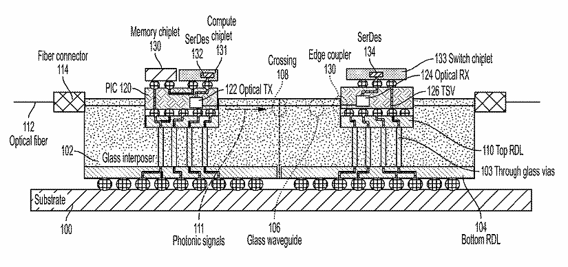
Figure 3: Optical communication substrate using glass interposer (Lightmatter, US20240353614).
Scaling-up to accommodate a plurality of photonic modules, the photonic system disclosed in the patent US12237871 (Figure 4) describes photonic interposers that enable efficient, high-bandwidth communication both within and between chips, using programmable photonic tiles arranged in 1D or 2D configurations. It also introduces a programmable physical network that connects these tiles via photonic links to enhance computing performance. Patent extensions have been filed in Europe and Asia, underscoring the significance of this invention for Lightmatter. A complementary patented invention with broad geographic IP protection, discloses an architecture that utilizes shared photomask sets (or at least one shared photomask) to manufacture multiple photonic modules on a single wafer (US11036002).
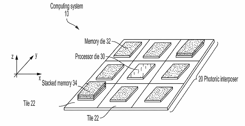
Figure 4: Photonic communication platform and related circuits (Lightmatter, US12237871).
Furthermore, the optical interposer and chiplets can be integrated within the same photonic package, as described in the invention claimed in patent US11947164. The photonic package includes a ceramic laminate substrate carrier with a recess that houses a photonic module, facilitating optical communication between electronic dies. Power delivery substrates provide electricity via bridge dies or interposers.
Outlook
Optical interposers are poised to revolutionize advanced semiconductor packaging to support AI and high-performance computing applications. By overcoming the limitations of traditional electrical interconnects, and offering high bandwidth, low latency, and energy-efficient data transmission, they are rapidly gaining traction in the semiconductor industry. Lightmatter’s robust patent portfolio and strategic partnerships underscores its ambition to strengthen its competitive advantage and leadership position in the photonic chip field, while demonstrating a clear vision for international market expansion. The company’s advancements in photonic computing, interconnects, and packaging solutions highlight the transformative potential of optical interposers in scaling AI applications. Its groundbreaking Passage™ platform, the world’s first 3D-stacked silicon photonics engine, connects thousands to millions of processors at the speed of light. This technology eliminates critical data bottlenecks, enabling unparalleled efficiency and scalability for the most advanced AI and high-performance computing workloads, thereby pushing the boundaries of AI infrastructure.
As the demand for high-speed, low-power computing solutions continues to surge, optical interposers will play a pivotal role in enabling next-generation architectures. Looking forward, Lightmatter’s proactive IP strategy and continued investment in innovation will be essential in shaping the future landscape of computing and maintaining leadership in an industry accelerating toward Artificial General Intelligence (AGI), a shift that demands exponentially greater computing performance and interconnect density.
Analyzing the technologies covered by patents held by key players offers valuable insights into their technological roadmaps, the future products they aim to bring to the market, their IP strategies, and the opportunities or risks they may represent.
To further explore and gain deeper insights into the technology trends and competitive landscape, feel free to contact us.
Press contact
contact@knowmade.fr
Le Drakkar, 2405 route des Dolines, 06560 Valbonne Sophia Antipolis, France
www.knowmade.com
About the author
Pauline Calka, PhD. works for KnowMade as a patent analyst in the fields of semiconductor manufacturing and advanced packaging. She holds a PhD in Memory from the University of Grenoble Alpes (France), in partnership with the CEA-Leti (France). After an Alexander von Humboldt Postdoc fellowship position at the Technical University of Berlin (Germany) and the Leibniz Institute for High Performance Microelectronics on ReRAM development, Pauline worked five years at ASM International (Belgium) as Senior Process Engineer on thin film development for logic, memory and MEMS, and two years at CEA-Leti as Integration Engineer on imaging CMOS sensors.
About KnowMade
KnowMade is a technology intelligence and IP strategy consulting company specialized in analyzing patents and scientific publications. The company helps innovative companies, investors, and R&D organizations to understand competitive landscape, follow technological evolutions, reduce uncertainties, and identify opportunities and risks in terms of technology and intellectual property.
KnowMade’s analysts combine their strong technology expertise and in-depth knowledge of patents with powerful analytics tools and methodologies to turn patent information and scientific literature into actionable insights, providing high added value reports for decision makers working in R&D, innovation strategy, intellectual property, and marketing. Our experts provide prior art search, patent landscape analysis, freedom-to-operate analysis, IP due diligence, and monitoring services.
KnowMade has a solid expertise in Compound Semiconductors, Power Electronics, Batteries, RF Technologies & Wireless Communications, Solid-State Lighting & Display, Photonics, Memories, MEMS & Sensors, Semiconductor Packaging, Medical Devices, Medical Imaging, Microfluidics, Biotechnology, Pharmaceutics, and Agri-Food.